Photodetector and spatial information detecting device using the same
A photoelectric detector, photoelectric conversion technology, applied in the direction of electric solid devices, circuits, electrical components, etc.
- Summary
- Abstract
- Description
- Claims
- Application Information
AI Technical Summary
Problems solved by technology
Method used
Image

Examples
no. 1 example
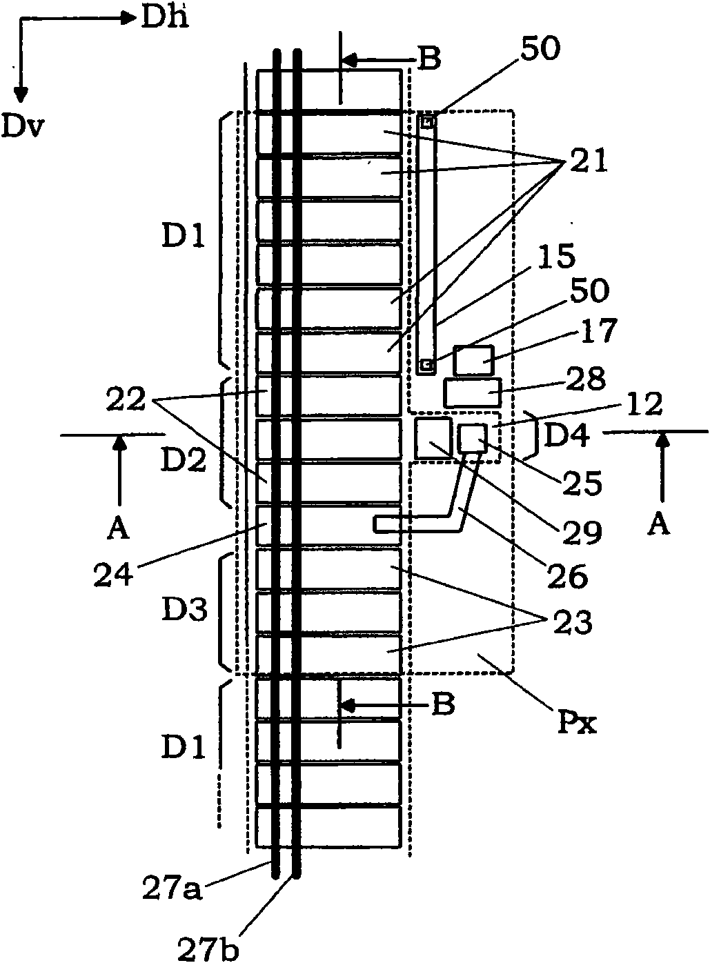
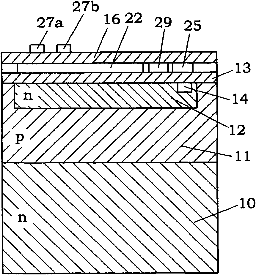
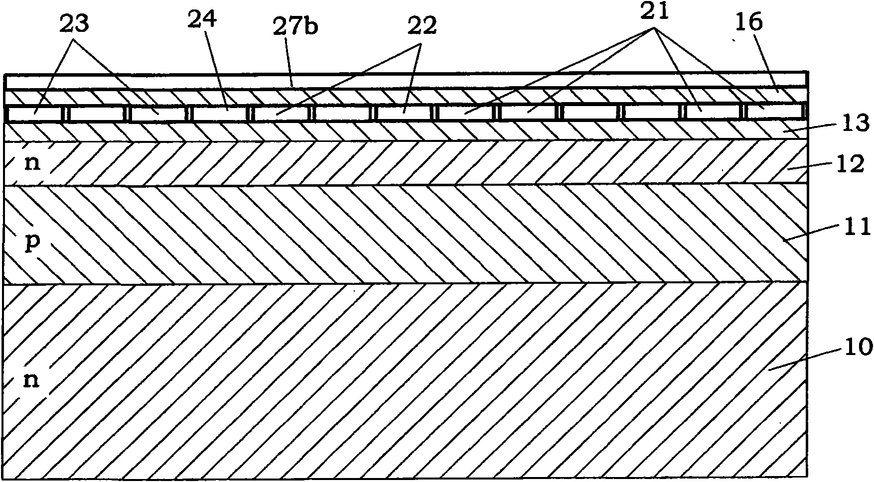
[0041] figure 1 A region corresponding to one pixel Px of the photodetector is shown. Such as figure 2 and image 3 As shown in , the pixel Px is provided with a substrate 10, a device formation layer 11 formed of a semiconductor material (for example, silicon) of a first conductivity type (for example, p-type) on the substrate 10, and a device formation layer 11 from the device formation layer 11. The overall surface (i.e., the upper surface) is formed at a required depth from a well 12 formed of a semiconductor material having a second conductivity type (for example, n type), formed on the overall surface of the well 12 and the overall surface of the device formation layer 11. An insulating layer 13 such as silicon oxide or silicon nitride, and electrodes provided on the insulating layer 13 . Such as image 3 As shown in , the electrodes include a sensitivity control electrode 21 , a separation electrode 22 , an accumulation electrode 23 and a barrier electrode 24 . In...
no. 2 example
[0101] The photodetector of the second embodiment is characterized in that the overflow drain region 15 (i.e., the charge removing portion) has a function of removing excess charge generated by the photoelectric conversion portion D1 when the amount of light received excessively increases, and removes the excess charge generated by the charge separating portion. Function of undesired charges separated by D2. When the excess charge is not removed, leakage of the excess charge to another pixel Px, a so-called image blooming phenomenon, may occur.
[0102] Incidentally, when the overflow drain region 15 is formed, as in the case of the first embodiment, there is a possibility that excess charges other than excess charges are lost from the photoelectric conversion portion D1 when removing undesired charges from the charge separation portion D2. charge. For example, when removing undesired charges in the period of collecting charges in the photoelectric conversion portion D1 by co...
no. 3 example
[0106] The photodetector of the third embodiment is characterized in that a pair of slit regions 32 is formed so as to straddle between the barrier electrode 24 in the well 12 and the adjacent separation electrode 22, as Figure 10 shown. In addition, the respective elongated regions 32 are spaced apart from each other in the horizontal direction Dh. That is, one of the elongated regions 32 is formed near one end of the barrier electrode 24 and the adjacent separation electrode 22, and the other elongated region 32 is formed near the opposite ends of the barrier electrode 24 and the adjacent separation electrode 22. nearby. For example, through ion implantation, each narrow region 32 is formed with a doping concentration higher than that of the n-type well 12. + conductivity type.
[0107] When the elongated region 32 is not formed, the potential gradually changes at the boundary portion of the well 12 . In other words, the boundary portion of the well 12 has a gradually r...
PUM
 Abstract
Description
Claims
Application Information
 - R&D
- Intellectual Property
- Life Sciences
- Materials
- Tech Scout
- Unparalleled Data Quality
- Higher Quality Content
- 60% Fewer Hallucinations
Browse by: Latest US Patents, China's latest patents, Technical Efficacy Thesaurus, Application Domain, Technology Topic, Popular Technical Reports.
© 2025 PatSnap. All rights reserved.Legal|Privacy policy|Modern Slavery Act Transparency Statement|Sitemap|About US| Contact US: help@patsnap.com