Display module assembly and method for fixing circuit wafer thereof

A technology of display module and fixing method, applied in printed circuit parts, optics, instruments, etc., can solve problems such as increasing the cost of eliminating EMI materials, electromagnetic interference, and reducing production efficiency

Active Publication Date: 2009-11-11
AU OPTRONICS (SUZHOU) CORP LTD +1
View PDF0 Cites 15 Cited by
  • Summary
  • Abstract
  • Description
  • Claims
  • Application Information

AI Technical Summary

Problems solved by technology

[0003] At present, the fixing structure of PCB is mostly fixed by screws. By opening holes on the PCB and locking with screws, the PCB can be effectively fixed, and the PCB is connected to the metal parts or the backplane through screws to solve the grounding problem, but this method needs to be increased. The cost of screw locking prolongs the assembly man-hours of the liquid crystal display device and reduces the production efficiency, especially when multiple screws are locked, it is easy to miss the locking screw phenomenon
And even if only a few screws are not locked to the PCB, it will make the PCB not evenly locked to the backplane
This will result in a decrease in product quality, leading to a decrease in yield
In addition, if the PCB board is placed on the side of the LCD module, it will increase the difficulty of screw locking, the metal parts also need to be designed with tapping, and the disassembly and assembly work takes a long time, and it is easy to damage the components
[0004] In addition, if the positioning method of the hook is used to fix the PCB, although this method is more convenient to operate, it may cause electromagnetic interference (Electro Magnetic Interference, EMI), but it also needs to increase the cost of materials to eliminate EMI

Method used


Image

  • Display module assembly and method for fixing circuit wafer thereof
  • Display module assembly and method for fixing circuit wafer thereof
  • Display module assembly and method for fixing circuit wafer thereof

Examples


Embodiment Construction

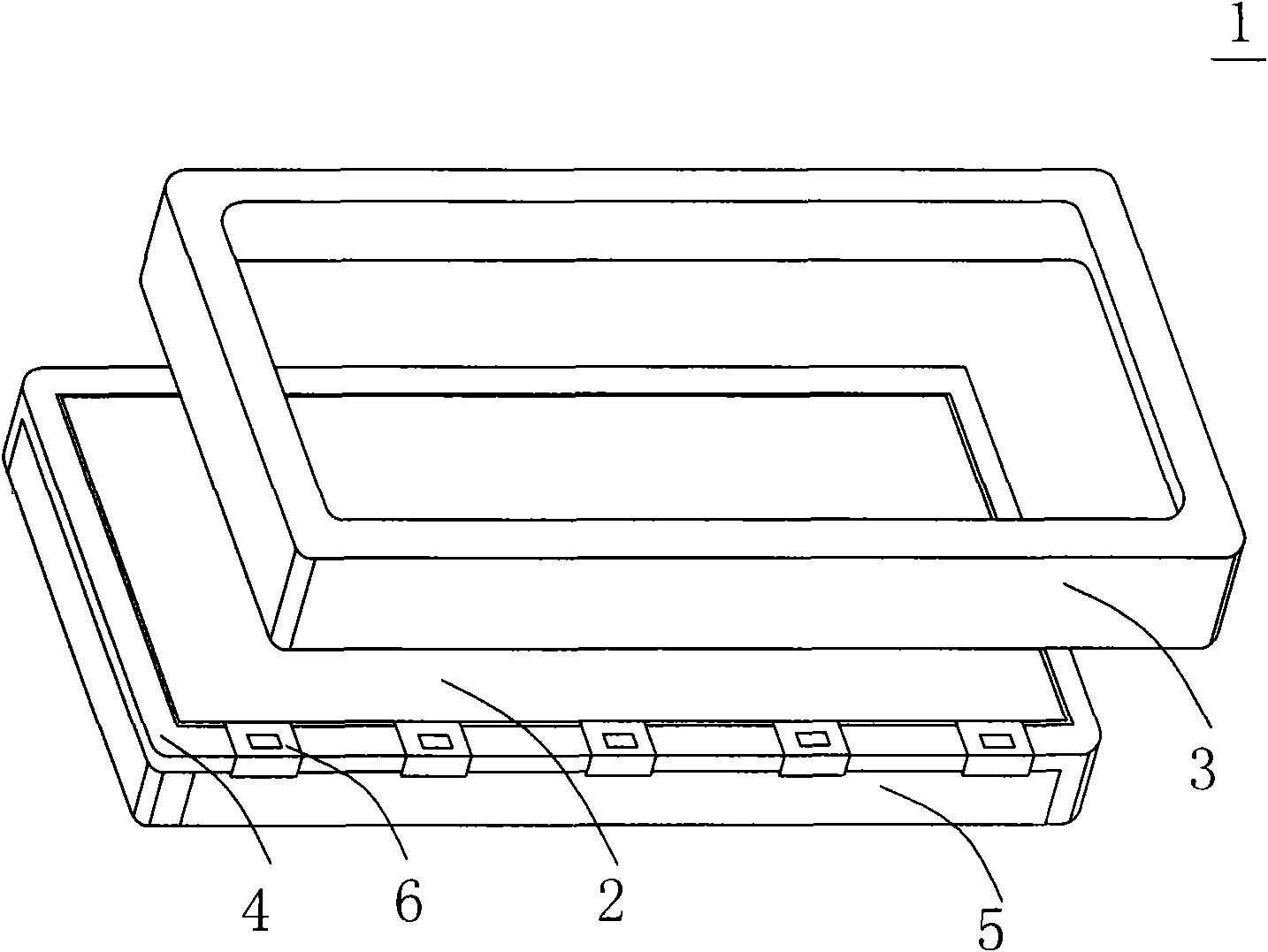
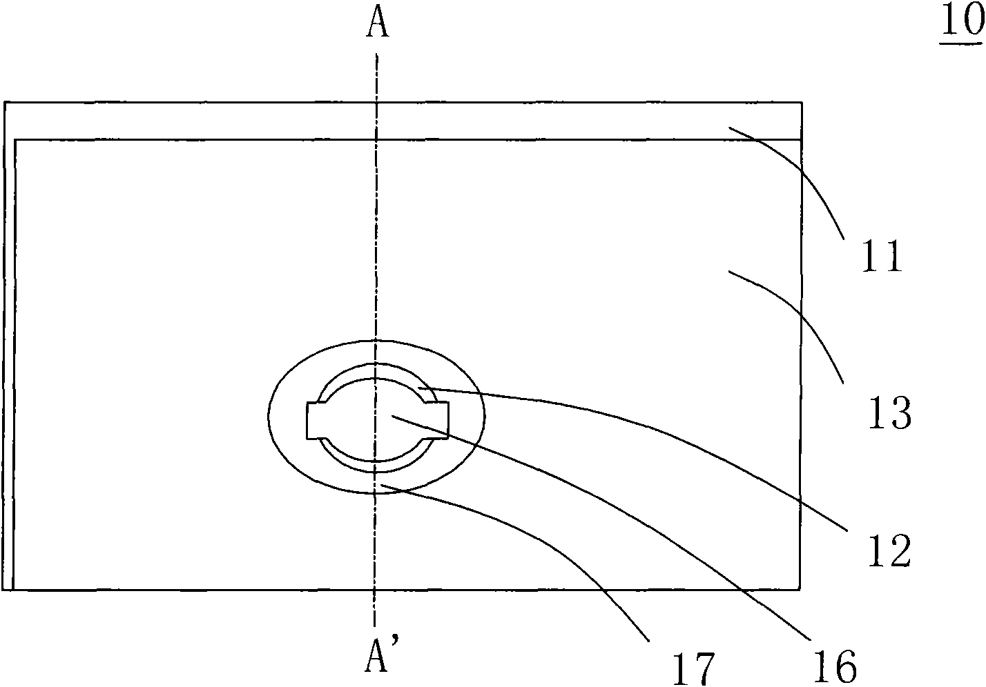
[0025] See figure 2 , image 3 with Figure 4 , figure 2 Shown is a partial schematic diagram of the display device according to the present invention, image 3 Shown is a schematic diagram of a circuit board according to the present invention, Figure 4 Shown as figure 2 A schematic cross-sectional view of the display device along the line A-A'. The display module 10 of the present invention includes a back plate 11, at least one fixing component 12 and a circuit board 13. Each fixing assembly 12 has a pair of connecting pieces 14 arranged on the back plate 11 and a pair of buckling pieces 15 respectively disposed on the connecting pieces, and the connecting pieces 14 of each fixing assembly 12 maintain a first distance D1, and The connecting members 14 of each fixing assembly 12 are adapted to be flexibly deformed in a manner of reducing the first distance D1. Wherein, the fixing component 12 is integrally formed with the back plate 11, or is made of the same material as the ...


PUM


Abstract

The invention provides a display module assembly and a method for fixing a circuit wafer thereof; wherein, the display module assembly comprises a backboard, at least a fixed component and the circuit wafer; the fixed components are provided with a pair of connecting pieces arranged at the backboard and a pair of fasteners arranged at the connecting pieces; a first distance is kept between the connecting pieces of the fixed components; and the connecting pieces of the fixed components are suitable to deform in a flexible way by means of shortening the first distance. The circuit wafer is provided with at least a fixed hole, the connecting pieces of the fixed components penetrate through one of the fixed holes and the fixed holes are restricted between the fasteners and the backboard of the corresponding fixed components.

Description

Technical field [0001] The invention relates to a method for fixing a circuit board, and in particular to a method for fixing a circuit board of a display module. Background technique [0002] The liquid crystal display module usually includes a liquid crystal display panel, a backlight module, and a plurality of frames for fixing the liquid crystal display panel and the backlight module. See figure 1 , figure 1 Shown is a schematic structural diagram of a liquid crystal display module in the prior art. The existing liquid crystal display module 1 includes a liquid crystal display panel 2, a back plate 5, a plastic frame 4, a front iron frame 3, and a printed circuit board (PCB) 6 , The liquid crystal display panel 2 includes a first substrate, a second substrate, and a liquid crystal layer (not shown in the figure) arranged between the first substrate and the second substrate, and the plastic frame 4 is fixed on the back by a clamping member or the like. On the board 5, the fr...

Claims


Application Information

Patent Timeline
Patent Type & Authority Applications(China)
IPC IPC(8): G02F1/13H05K1/02
Inventor 包振毅
Owner AU OPTRONICS (SUZHOU) CORP LTD
Why Eureka
Try Eureka