Polishing apparatus

A technology of equipment and polishing liquid, which is used in grinding/polishing equipment, metal processing equipment, machine tools for surface polishing, etc. question

Inactive Publication Date: 2009-11-25
EBARA CORP
View PDF0 Cites 15 Cited by
  • Summary
  • Abstract
  • Description
  • Claims
  • Application Information

AI Technical Summary

Problems solved by technology

In addition, the non-uniformity of the polishing profile due to the inclination of the retaining ring increases with the equalization of the rotation of the semiconductor wafer
[0012] However, traditional snap rings are difficult to improve the temperature of the polishing pad and the controllability of the polishing profile

Method used


Image

  • Polishing apparatus
  • Polishing apparatus
  • Polishing apparatus

Examples


Embodiment Construction

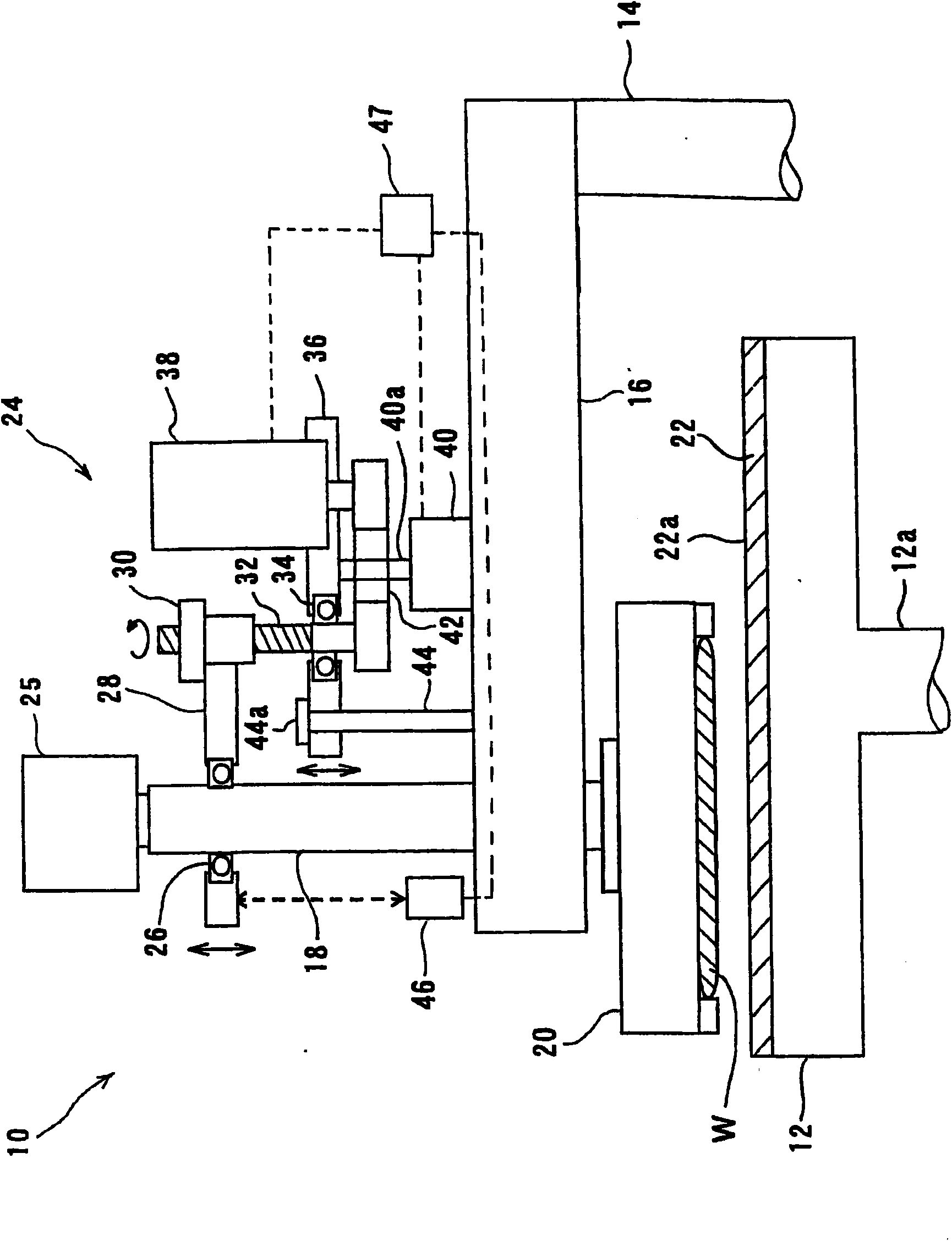
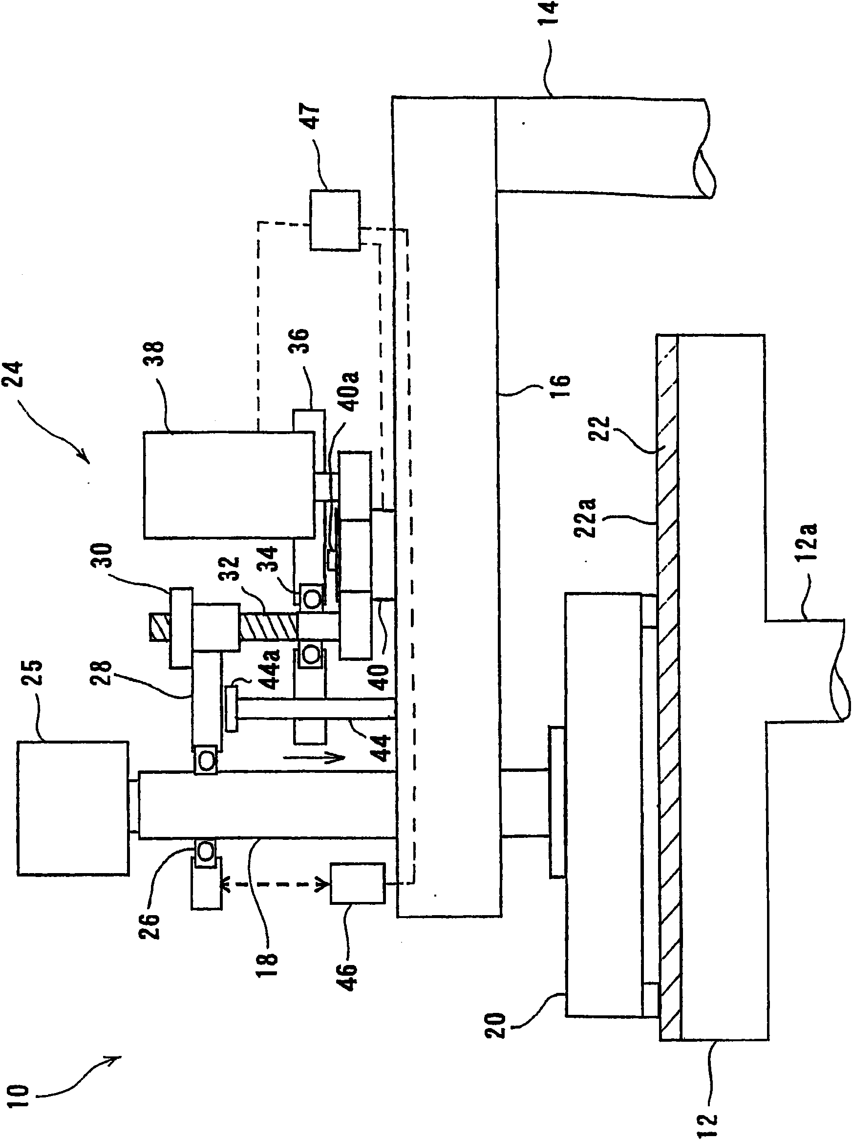
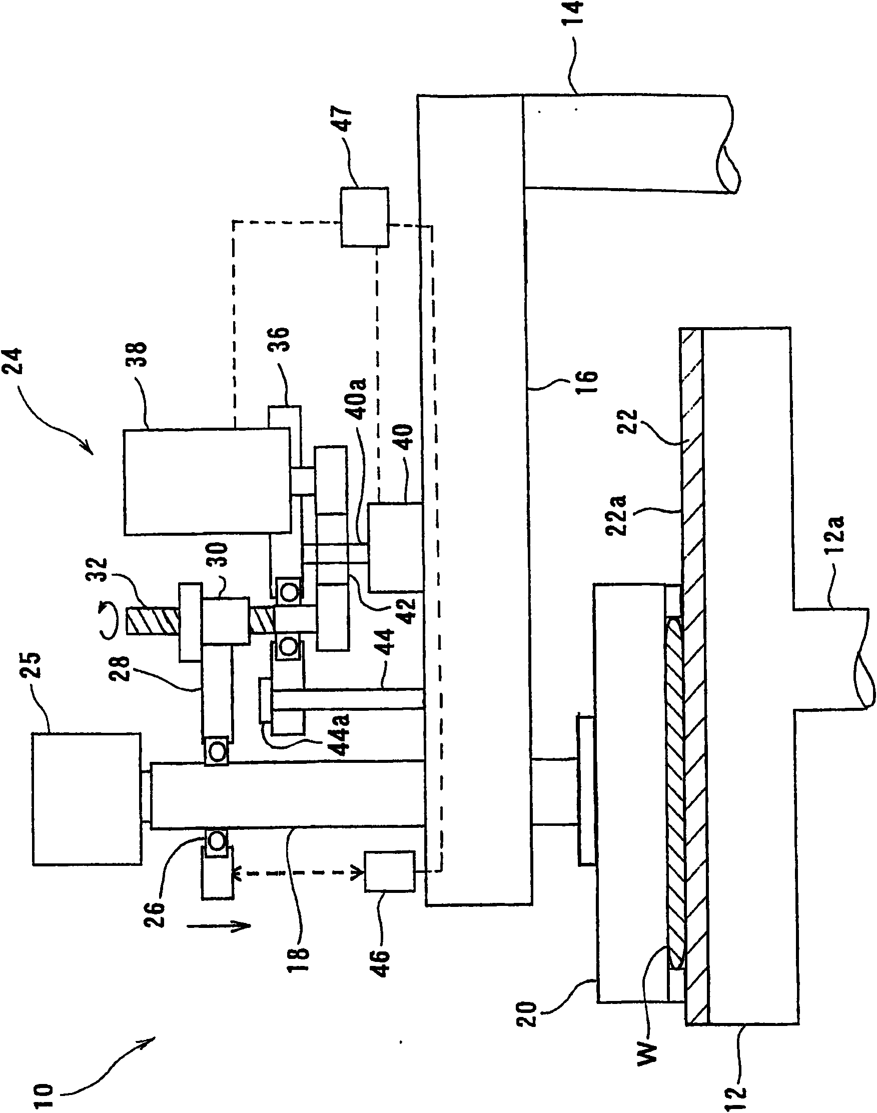
[0074] The following will refer to Figure 1 to Figure 32 An embodiment of the polishing apparatus according to the present invention is described. Like or corresponding parts are indicated with like or corresponding reference numerals throughout the drawings and will not be repeated below.

[0075] figure 1 is a schematic diagram showing a polishing apparatus 10 according to a first embodiment of the present invention. like figure 1 As shown, polishing apparatus 10 has polishing table 12 , top ring head 16 connected to the upper end of support shaft 14 , top ring shaft 18 mounted on the free end of top ring head 16 , and top ring 20 connected to the lower end of top ring shaft 18 . In the example shown, the top ring 20 is substantially in the form of a circular plate.

[0076] The polishing table 12 is connected to a motor (not shown) placed below the polishing table 12 via a table shaft 12a. Therefore, the polishing table 12 can rotate around the table axis 12a. like ...


PUM


Abstract

A polishing apparatus (1) has a polishing pad (22), a top ring (20) for holding a semiconductor wafer (W), a vertical movement mechanism (24) operable to move the top ring (20) in a vertical direction, a distance measuring sensor (46) operable to detect a position of the top ring (20) when a lower surface of the top ring (20) is brought into contact with the polishing pad (22), and a controller (47) operable to calculate an optimal position of the top ring (20) to polish the semiconductor wafer (W) based on the position detected by the distance measuring sensor (46). The vertical movement mechanism (24) includes a ball screw mechanism (30, 32, 38, 42) operable to move the top ring (20) to the optimal position.

Description

technical field [0001] This application is a divisional application based on the patent application 200580037559.0 (PCT / JP2005 / 020334) submitted on October 31, 2005. [0002] This invention relates to polishing apparatus, and more particularly to polishing apparatus for polishing substrates, such as semiconductor wafers, into flat, mirror-finished pieces. Background technique [0003] In recent years, semiconductor devices have become more integrated, and the structure of semiconductor elements has become more complicated. In addition, the number of layers in the multilayer interconnect for logic systems has also increased. Therefore, irregularities on the surface of the semiconductor device increase, so that the height of the steps on the surface of the semiconductor device tends to become large. This is because, in the semiconductor device manufacturing process, first a thin film is formed on the semiconductor device, then a micromachining process such as forming a patte...

Claims


Application Information

Patent Timeline
Patent Type & Authority Applications(China)
IPC IPC(8): B24B29/00H01L21/304B24B49/02B24B53/12B24B41/047B24B37/07B24B37/10B24B37/32B24B49/10B24B49/12B24B49/16
Inventor 锅谷治户川哲二福岛诚安田穗积
Owner EBARA CORP
Why Eureka
Try Eureka