Light-emitting diode structure

A technology of light-emitting diodes and bases, which is applied to semiconductor devices of light-emitting elements, light sources, cooling/heating devices of lighting devices, etc., and can solve problems such as small contact area, affecting the luminous efficiency and life of light-emitting diodes, and poor heat dissipation

Inactive Publication Date: 2009-11-25
FU ZHUN PRECISION IND SHENZHEN +1
View PDF0 Cites 4 Cited by
  • Summary
  • Abstract
  • Description
  • Claims
  • Application Information

AI Technical Summary

Problems solved by technology

In this light-emitting diode structure, the contact area between the base 22 and the air is small, and its heat dissipation effect is not good, which further affects the luminous efficiency and life of the light-emitting diode.

Method used


Image

  • Light-emitting diode structure
  • Light-emitting diode structure

Examples


Embodiment Construction

[0010] The present invention will be further described below in conjunction with specific embodiments with reference to the accompanying drawings.

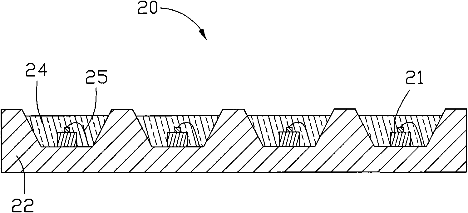
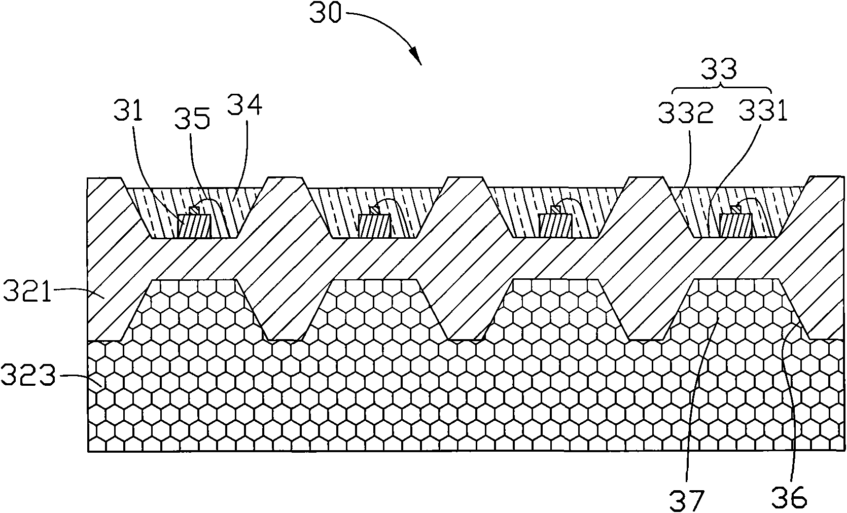
[0011] figure 2 Shown is a schematic diagram of the light emitting diode structure in an embodiment of the present invention. The light emitting diode structure 30 includes a base 321, a plurality of light emitting diode chips 31 on the base 321, packages 34 respectively fixing the light emitting diode chips 31 on the base 321, and a heat sink under the base. Board 323.

[0012] The upper surface of the base 321 is recessed downwards to form several bowl-shaped packaging cavities 33 . Each packaging cavity 33 has a horizontal bottom surface 331 and side surfaces 332 inclined upwards and outwards from the bottom surface 331 . The light-emitting diode chips 31 are arranged on the bottom surface 331 of the package cavity 33 in one-to-one correspondence, and are electrically connected to the conductive components (not shown) on th...


PUM


Abstract

The invention relates to a light-emitting diode structure comprising a base, at least one light-emitting diode chip and an encapsulation body, wherein the light-emitting diode chip is arranged on the base, and the encapsulation body is used for protecting the light-emitting diode chip. A heat radiation plate is attached below the base and has a porous structure in which a plurality of hole gaps are formed. In the light-emitting diode structure, because the inside of the heat radiation plate is provided with the hole gaps, the contact area of the heat radiation plate and air can be greatly increased, thermal resistance is reduced, thermal convection performance is enhanced, and heat generated by the light-emitting diode chip can be rapidly dispersed by the heat radiation plate after being absorbed by the base and transmitted to the heat radiation plate.

Description

technical field [0001] The invention relates to a light emitting diode structure. Background technique [0002] Light Emitting Diode (Light Emitting Diode) uses the change of energy band level when electrons and holes in semiconductor materials are combined to release energy in the form of light. Because light-emitting diodes have the advantages of small size, long life, low driving voltage, fast response speed, and good shock resistance, they have been widely used in various fields such as advertising boards, traffic signs, and daily lighting. [0003] figure 1 A typical LED structure 20 is shown, including a base 22 , a plurality of LED chips 21 on the base 22 and an encapsulant 24 surrounding the LED chips 21 . The light emitting diode chip 21 is electrically connected to a conductive component (not shown) on the base 22 through a wire 25 . The base 22 is a metal plate with a flat lower surface, and the heat generated by the LED chip 21 is first dissipated through the ...

Claims


Application Information

Patent Timeline
Patent Type & Authority Applications(China)
IPC IPC(8): H01L25/075H01L23/367H01L23/373H01L23/13H01L33/00
CPCH01L25/0753F21K9/00H01L2224/45144H01L2224/48091F21V29/763F21V29/89H01L33/641H01L2924/00014H01L2924/00
Inventor 魏百盛张家寿
Owner FU ZHUN PRECISION IND SHENZHEN
Why Eureka
Try Eureka