Thin film transistor (TFT) substrate, manufacturing method thereof and display device

A thin film transistor and substrate technology, applied in the field of electrowetting display devices, can solve the problems of poor optical quality and complex structure, and achieve the effects of simple structure, convenient use and good optical quality

Inactive Publication Date: 2009-12-02
INNOCOM TECH SHENZHEN +1
View PDF0 Cites 7 Cited by
  • Summary
  • Abstract
  • Description
  • Claims
  • Application Information

AI Technical Summary

Problems solved by technology

[0011] In order to solve the problems of complex structure and poor optical quality in the prior art, it is necessary to provide an electrowetting display device with simple structure and better optical quality

Method used


Image

  • Thin film transistor (TFT) substrate, manufacturing method thereof and display device
  • Thin film transistor (TFT) substrate, manufacturing method thereof and display device
  • Thin film transistor (TFT) substrate, manufacturing method thereof and display device

Examples


Embodiment Construction

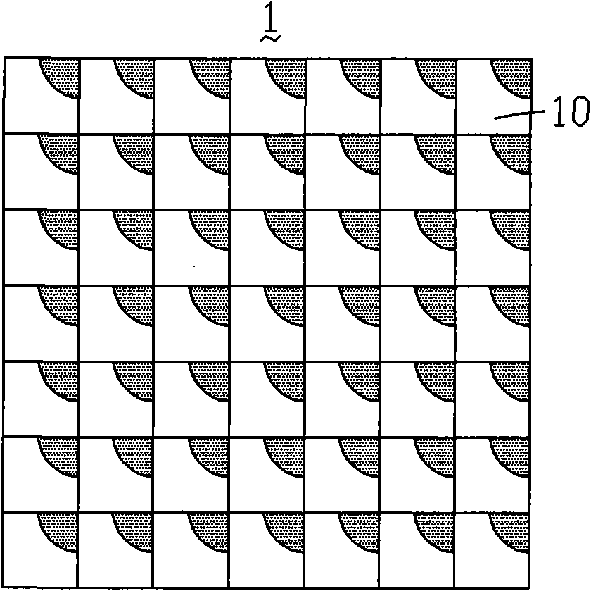
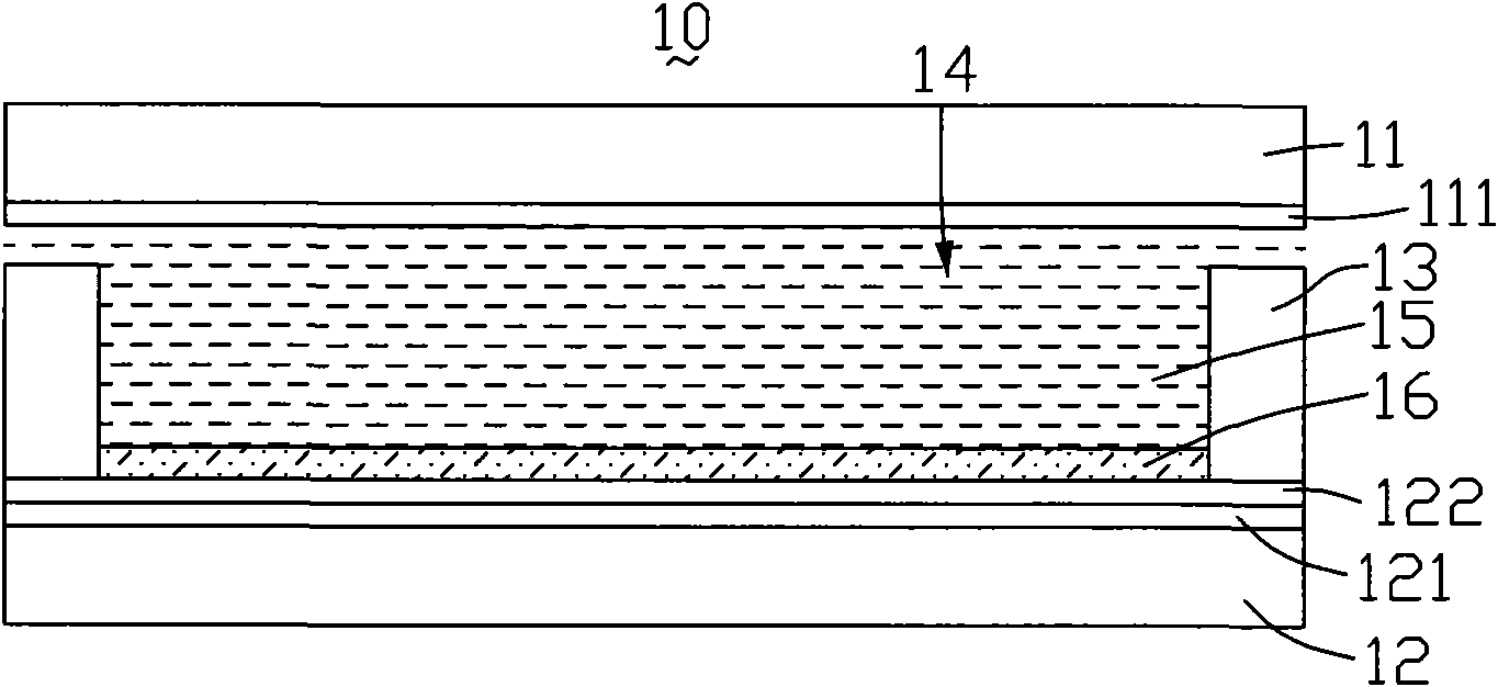
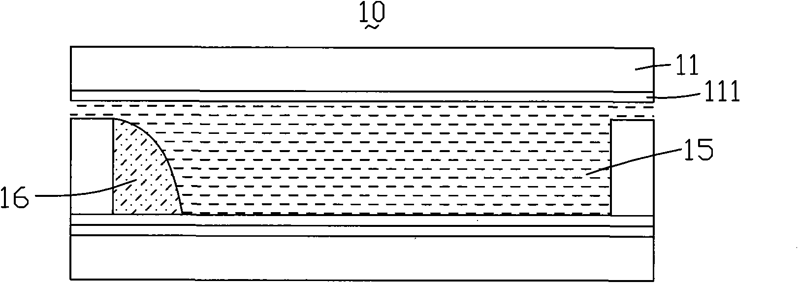
[0035] see Figure 4 , is a partial structural schematic diagram of the first embodiment of the electrowetting display device of the present invention. The electrowetting display device 4 is a transmissive display device, which includes a facing substrate 41, a thin film transistor substrate 42 opposite to the facing substrate 41, and a thin film transistor substrate 42 located between the facing substrate 41 and the thin film transistor substrate 42. The sealant 49 between them, a plurality of intersecting partitions 43 between the opposite substrate 41 and the thin film transistor substrate 42 arranged in rows and columns, and a backlight module (not shown) adjacent to the thin film transistor substrate 42 . The TFT substrate 42 includes a frame glue setting area (not shown). The frame glue 49 is arranged in the frame glue setting area and abuts the two substrates 41, 42 and cooperates with the two substrates 41, 42 to form a closed first receiving space 441, and the frame...


PUM


Abstract

The invention provides a thin film transistor (TFT) substrate, a manufacturing method thereof and an electro-wetting type display device. The TFT substrate comprises a display area, at least one contact area which is positioned on at least one side of the display area, a frame adhesive arranging area which surrounds the display area and the contact area and is used for arranging frame adhesive, a plurality of pixel electrodes which are arranged in the display area and at least one public electrode which is arranged in the contact area. In addition, the TFT substrate is exposed out of at least part of the public electrode.

Description

technical field [0001] The invention relates to a thin film transistor substrate, a manufacturing method of the thin film transistor substrate and an electrowetting display device. Background technique [0002] Nowadays, many optoelectronic technologies are developing rapidly and applied to the next generation flat panel display, such as projection display (Projection Display), flexible display (FlexibleDispaly) and so on. In this environment, a display device based on the principle of electrowetting has attracted extensive attention due to its advantages such as fast response speed, wide viewing angle, low power consumption, light weight and portability. [0003] see figure 1 , is a schematic plan view of a reflective display device based on the principle of electrowetting disclosed in the prior art. The display device 1 includes a plurality of pixels 10 arranged in a matrix, and the pixels 10 are controlled to display different gray scales to form a picture required to b...

Claims


Application Information

Patent Timeline
IPC IPC(8): H01L27/12H01L21/84H01L21/768G02B26/02
Inventor 李睿匀颜硕廷黄荣龙
Owner INNOCOM TECH SHENZHEN
Why Eureka
Try Eureka