Forming method of groove

A technology of trench and dry etching, which is applied in the fields of electrical components, semiconductor/solid-state device manufacturing, circuits, etc., can solve the problems affecting the efficiency of semiconductor manufacturing process, many process steps, and long time spent, so as to reduce the cost of semiconductor manufacturing The effect of process steps, reduction of process steps, and improvement of efficiency

Active Publication Date: 2009-12-09
SEMICONDUCTOR MANUFACTURING INTERNATIONAL (BEIJING) CORP
View PDF1 Cites 13 Cited by
  • Summary
  • Abstract
  • Description
  • Claims
  • Application Information

AI Technical Summary

Problems solved by technology

[0008] The existing process of forming a sub-trench includes forming a spacer layer 112 on the surface of the gate layer 104 and in the first-type trench 110, defining the shape of the sub-trench 114 on the sidewall layer 112, and then forming a spacer layer 112 on the sidewall layer 112. 112 is a mask, etch the insulating dielectric layer 108 to the required depth to form a sub-trench 114, and finally remove the sidewall layer 112, which requires many steps such as deposition, photolithography, etching, wet cleaning, etc., so that the entire semiconductor manufacturing There are many process steps and it takes a long time, which affects the efficiency of the entire semiconductor manufacturing process

Method used


Image

  • Forming method of groove
  • Forming method of groove
  • Forming method of groove

Examples


Embodiment Construction

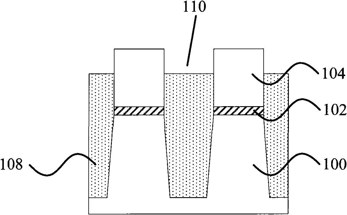
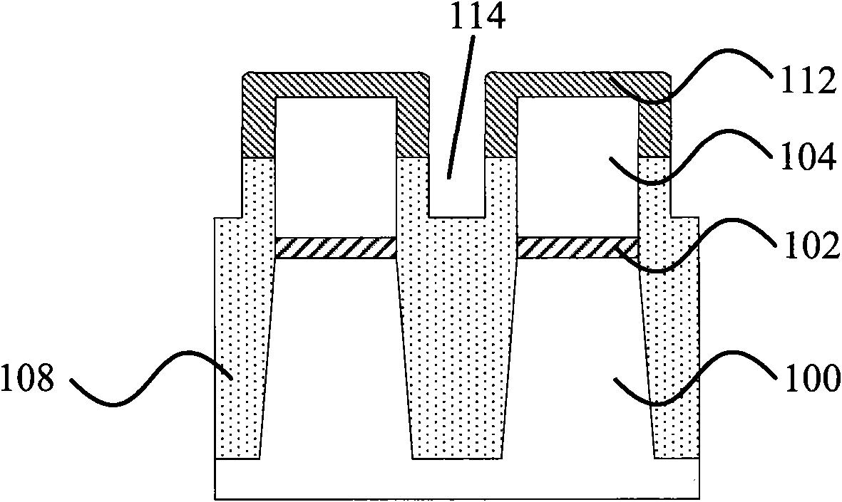
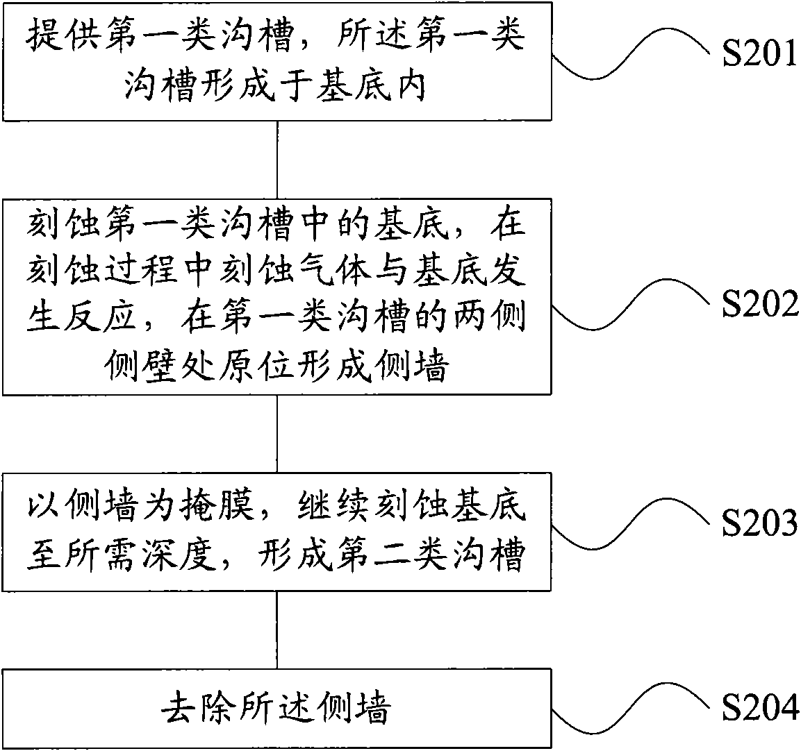
[0026] The present invention uses dry etching to etch the substrate in the first type of trench during the formation of the entire trench. During the etching process, the etching gas and the sidewalls of the first type of trench are combined with each other. The reaction product of the substrate is formed in situ as a mask sidewall for etching to form the second type of trench. The invention reduces the semiconductor manufacturing process steps, shortens the time spent in forming the entire trench, improves the efficiency of the entire semiconductor manufacturing process, and optimizes the process.

[0027] The present invention uses C 4 F 8 , C 4 F 6 , C 5 F 8 , CH 2 F 2 , C 5 F 10 Or an etching gas of any combination thereof to form the second type trench. In the process of etching the trench, it reacts with the substrate to form in-situ mask sidewall spacers for forming the second type trench by etching. The invention reduces the semiconductor manufacturing process steps, short...


PUM


Abstract

The invention relates to a forming method of a groove, which comprises the following steps: providing a first groove, wherein the first groove is formed in a base; etching a base in the first groove, wherein etching gases react with the base during the etching, home positions of two side walls of the first groove are provided with side walls; continuously etching the base until reaching the needed depth so as to form a second groove by using the side walls as a mask; and removing the side walls. Reaction products of the etching gases and the base at the two side walls of the first groove are formed into polymer side walls at the home positions in the process of dry-etching the base in the first groove, the polymer side walls replace multilayered medium layer side walls at two side walls of the first groove before the etching of the second groove and are used as a hard mask of continuously etching the second groove, thereby improving the efficiency of the semiconductor fabrication process and optimizing the process.

Description

Technical field [0001] The present invention relates to the technical field of semiconductor manufacturing, and in particular to a method for forming a trench. Background technique [0002] In the semiconductor manufacturing process, in order to form a trench of a desired shape on a semiconductor substrate, an etching method can be used to carve a trench of a desired position, size and depth in the semiconductor substrate. There are many ways to form trenches. The most common method is to pattern a mask layer (such as a photoresist layer or a silicon nitride layer), and expose the to-be-etched under the mask layer at the position where the trench needs to be formed. The material layer is etched, and then the mask layer remaining after patterning is used as a mask to etch the material layer to a desired depth to form a trench, and finally the mask layer is removed. [0003] In the actual process, the mask layer can also be more than one layer, and the materials, thickness, and for...

Claims


Application Information

Patent Timeline
Patent Type & Authority Applications(China)
IPC IPC(8): H01L21/00H01L21/02H01L21/311H01L21/768
Inventor 杨芸洪中山
Owner SEMICONDUCTOR MANUFACTURING INTERNATIONAL (BEIJING) CORP
Why Eureka
Try Eureka