
Organic light emitting device, method of manufacturing the same, display unit, and electronic device

A technology for organic light-emitting devices and manufacturing methods, which are applied in semiconductor/solid-state device manufacturing, electrical solid-state devices, semiconductor devices, etc., can solve problems such as insufficient electrical connection, and achieve the effects of suppressing brightness fluctuation, good display quality, and suppressing voltage drop

Inactive Publication Date: 2009-12-09
SONY GRP CORP
View PDF3 Cites 31 Cited by
  • Summary
  • Abstract
  • Description
  • Claims
  • Application Information

AI Technical Summary

Problems solved by technology

Therefore, there is a possibility that the electrical connection between the auxiliary wiring and the second electrode is insufficient

Method used


Image

  • Organic light emitting device, method of manufacturing the same, display unit, and electronic device
  • Organic light emitting device, method of manufacturing the same, display unit, and electronic device
  • Organic light emitting device, method of manufacturing the same, display unit, and electronic device

Examples


no. 1 example

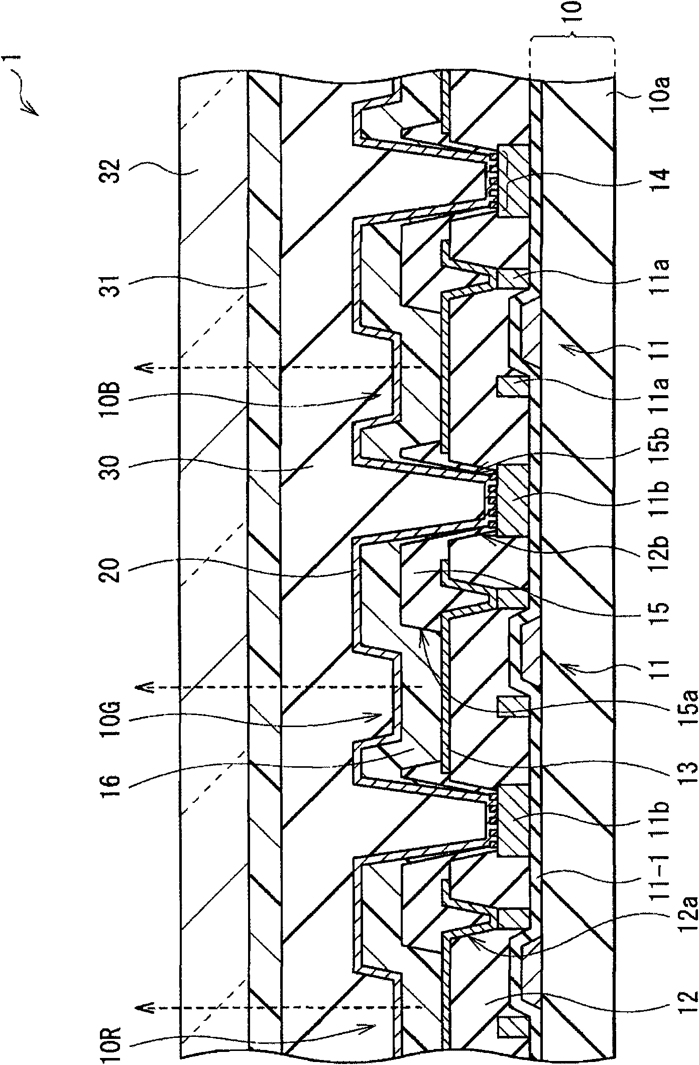
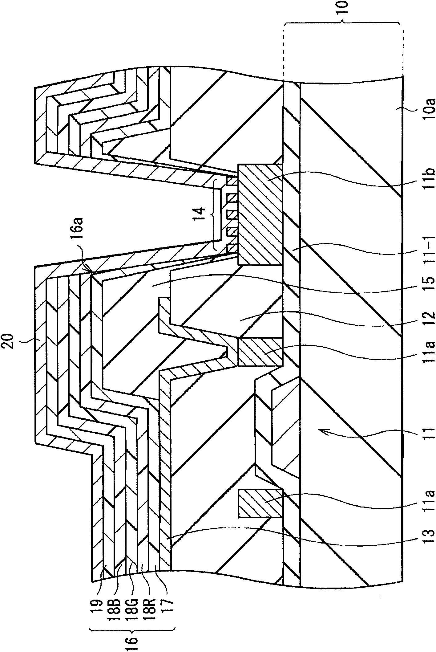
[0047] figure 1 A cross-sectional structure of the display unit 1 of the first embodiment of the present invention is shown. The display unit 1 is suitably used as a thin organic light emitting display in which the driving board 10 and the sealing board 32 are arranged oppositely, and the entire areas of the driving board 10 and the sealing board 32 are covered with a film made of, for example, a thermosetting resin. The adhesive layer 31 is bonded together. In the driving board 10, for example, an organic light-emitting device 10R generating red light, an organic light-emitting device 10R generating green light, and an organic light-emitting device 10R generating green light are arranged sequentially in a matrix state as a whole via a TFT 11 and a planarizing layer 12 over a substrate 10a of an insulating material such as glass. A light emitting device 10G and an organic light emitting device 10B generating blue light.

[0048] The TFT 11 is a driving element corresponding ...

no. 2 example

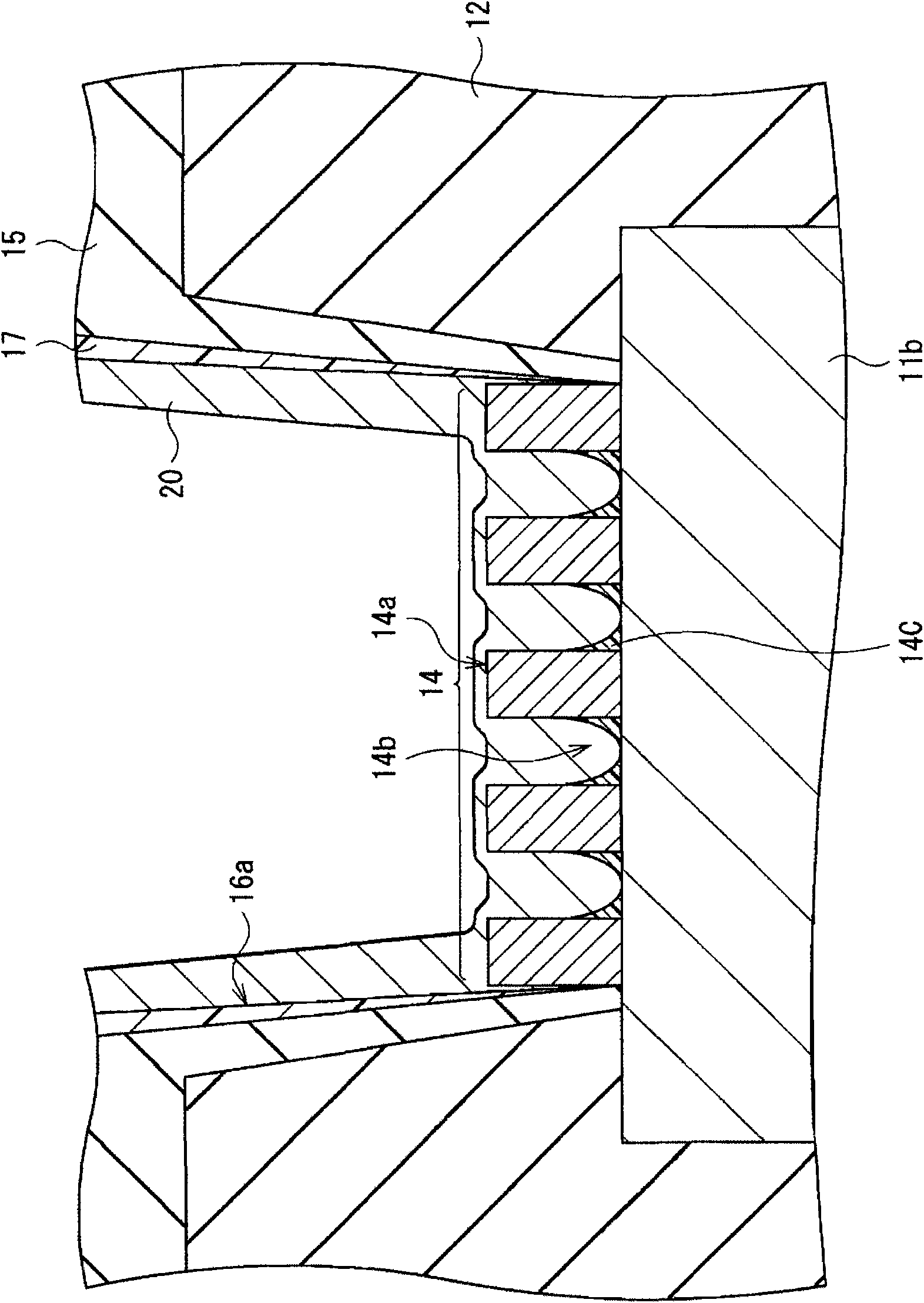
[0091] Figure 12 An enlarged view of a region where the connection portion 14 in the display unit of the second embodiment of the present invention is formed is shown. This embodiment has a structure similar to that of the first embodiment except that the structure of the organic layer 23c is different. Therefore, the same elements as those of the first embodiment are denoted by the same reference numerals, and descriptions thereof are appropriately omitted.

[0092] An organic layer 23 c is formed at the bottom surface of the concave portion 14 b of the connection portion 14 . The organic layer 23c contains, for example, conductive fine particles in addition to the constituent materials of the above-mentioned organic layer 16 . The second electrode 20 is formed so as to cover the organic layer 23c and the convex portion 14a. Examples of conductive fine particles include metal fine particles such as gold, silver, and aluminum, conductive fine particles such as ITO and ZnO,...


PUM


Abstract

An organic light emitting device capable of securing favorable electric connection between an auxiliary wiring layer and a second electrode without using a pixel separation mask, a method of manufacturing the same, a display unit, and an electronic device are provided. In the organic light emitting devices, for example, the auxiliary wiring layer, a first electrode as an anode, an insulating film between pixels, an organic layer including a light emitting layer, and the second electrode as a cathode are formed in this order over a substrate. In a region of the organic layer corresponding to the auxiliary wiring layer, an aperture is provided. On the auxiliary wiring layer, a connection section having a plurality of convex sections is formed. In the aperture of the organic layer, the auxiliary wiring layer and the second electrode are electrically connected by the connection section.

Description

[0001] Cross References to Related Applications [0002] The present application contains subject matter related to the disclosure of Japanese Priority Patent Application JP 2008-149263 filed in the Japan Patent Office on Jun. 6, 2008, the entire content of which is hereby incorporated by reference. technical field [0003] The present invention relates to an organic light emitting device provided with, for example, auxiliary wiring for suppressing a voltage drop, a method of manufacturing the organic light emitting device, a display unit and an electronic device using the organic light emitting device. Background technique [0004] In recent years, organic light emitting displays using organic light emitting devices have attracted attention. In an organic light emitting device, a first electrode, an organic layer including a light emitting layer, and a second electrode are sequentially stacked over a substrate. As the material of the organic layer, low-molecular materials ...

Claims


Application Information

Patent Timeline
Patent Type & Authority Applications(China)
IPC IPC(8): H01L51/50H01L51/52H01L51/56H01L27/32H01L23/522H01L21/768
CPCH01L27/3276H10K59/131H10K59/80522Y10S428/917H10K59/35H10K50/824
Inventor 花轮幸治
Owner SONY GRP CORP
Learn More