Wafer supporting device and etching device

A wafer carrying and wafer technology, which is applied in the manufacture of discharge tubes, electrical components, semiconductor/solid-state devices, etc., can solve the problems of damage to the focus ring 122, deterioration of etching uniformity, and impact on focusing performance, etc., to increase the use of The effect of life, improving yield and prolonging service life

Inactive Publication Date: 2010-01-06
SEMICONDUCTOR MANUFACTURING INTERNATIONAL (BEIJING) CORP
View PDF0 Cites 8 Cited by
  • Summary
  • Abstract
  • Description
  • Claims
  • Application Information

AI Technical Summary

Problems solved by technology

However, since the focus ring 124 is arranged on the flat surface 1240 of the insulating ring 124, during the plasma sputtering process, the edge of the focus ring 124 will be directly eroded by the plasma. Regression into an arc (such as Figure 2b shown), damage the focus ring 122 and affect its service life
In addition, as the edge of the focus ring 122 gradually wears out, the remaining flat part of the focus ring 122 will continue to shrink inward and become smaller, affecting its focusing performance, resulting in changes in the etching rate of the edge of the wafer W, resulting in The etching rate at the center of the wafer is the same as that at the outer edge of the wafer, and the etching uniformity becomes worse

Method used


Image

  • Wafer supporting device and etching device
  • Wafer supporting device and etching device
  • Wafer supporting device and etching device

Examples


Embodiment Construction

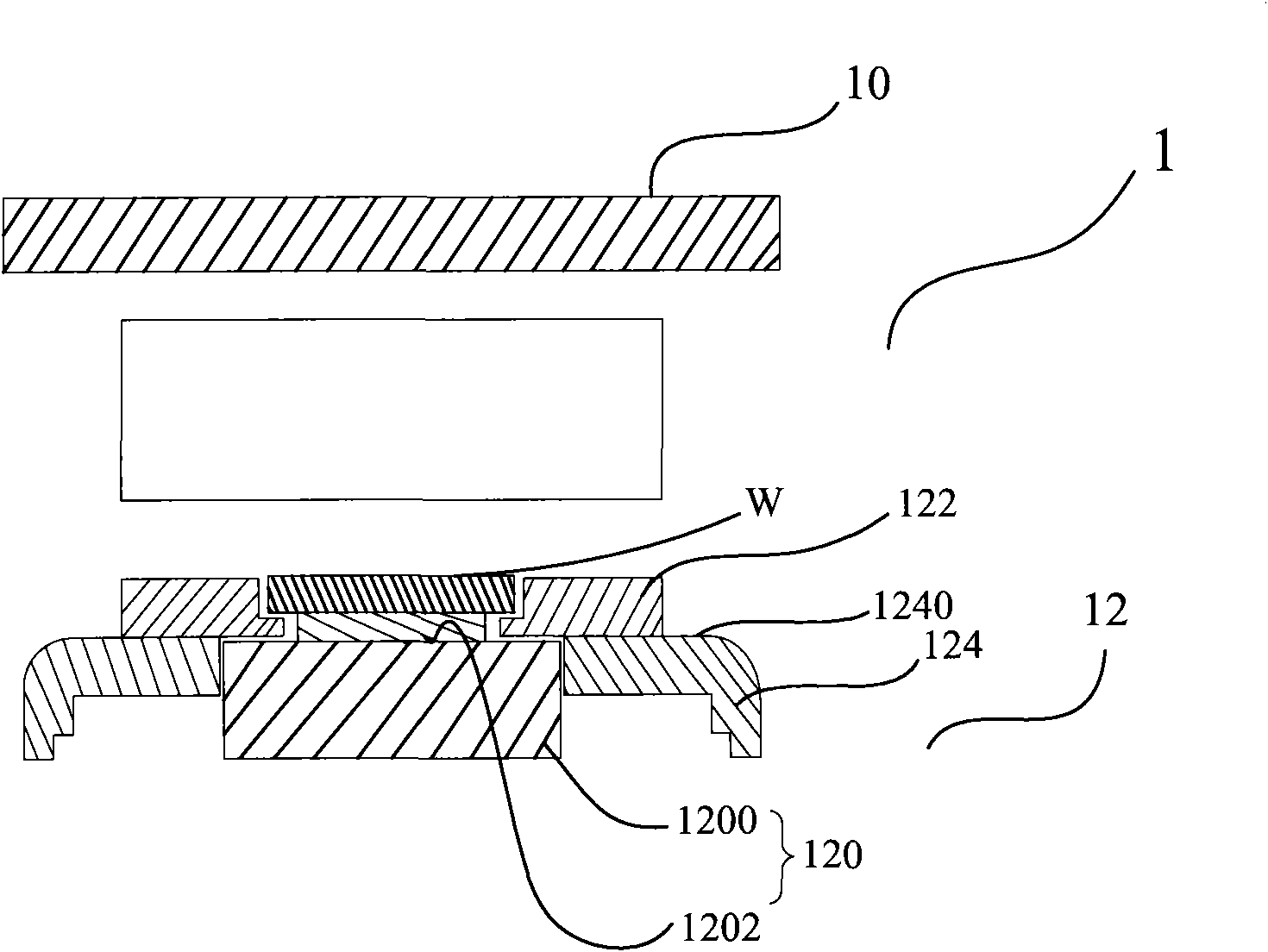
[0022] The present invention provides a wafer carrier device applied to a semiconductor manufacturing process, comprising an electrostatic chuck, a focus ring and an insulating member, wherein the surface of the insulating member has a first section and a second protrusion protruding from the first section. section. Embodiments of the present invention will be described below by taking an etching apparatus for wafer etching processing as an example with reference to the accompanying drawings.

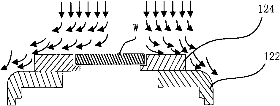
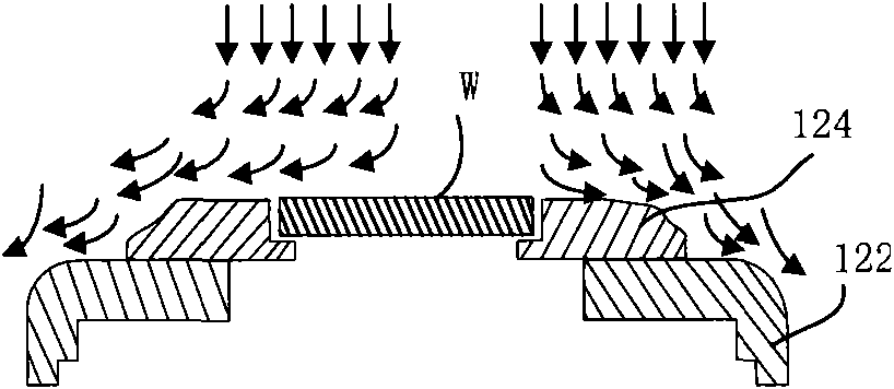
[0023] image 3 It is a longitudinal cross-sectional side view of an embodiment of the etching apparatus of the present invention. like image 3 As shown, the etching apparatus 3 may include a hermetic processing vessel (not shown) that is grounded. The airtight processing container includes an upper electrode 30 and a wafer carrier 32 disposed opposite to the upper electrode 30 . Among them, the upper electrode 30 is an etching gas (for example, including C 4 F 8 gas, C 5 F 8 G...


PUM


Abstract

The invention relates to a wafer supporting device, which comprises a wafer holder, a focusing ring and an insulating member arranged on the wafer holder. The surface of the insulating member is provided with a first section and a second section. The second section can be aligned with the focusing ring. By adopting the insulating member with an improved structure, the wafer supporting device can avoid the damage of the focusing ring due to the fact the plasma generated in the semiconductor manufacturing process erodes the fringe of the focusing ring directly, reduce the loss of the focusing ring and the insulating member and prolong the service life. Furthermore, the invention can improve etching uniformity of a wafer in the etching process, and improve yield of the product correspondingly.

Description

technical field [0001] The invention relates to a wafer carrying device and an etching device. Background technique [0002] Plasma etching is generally performed in a plasma-generating processing apparatus. Such a processing apparatus has a reaction chamber for generating plasma in an atmosphere introduced with a processing gas including, for example, C, and processing the loaded wafers to be processed. 4 F 8 gas, C 5 F 8 Gas and trace O 2 gas. , in the reaction chamber, a carrier device with the function of an electrode for generating plasma and holding the wafer to be processed is arranged. [0003] figure 1 It is a longitudinal cross-sectional side view showing a conventional etching apparatus. like figure 1 As shown, the etching apparatus 1 has an upper electrode 10 and a wafer carrier 12 disposed opposite to the upper electrode 10 . The wafer carrier 12 includes a wafer stage 120 for holding the wafer W to be processed, a focus ring 122 surrounding the wafer ...

Claims


Application Information

Patent Timeline
Patent Type & Authority Applications(China)
IPC IPC(8): H01L21/683H01L21/687H01L21/00H01L21/02H01L21/3065H01J37/32C23F4/00
Inventor 陈文财
Owner SEMICONDUCTOR MANUFACTURING INTERNATIONAL (BEIJING) CORP
Why Eureka
Try Eureka