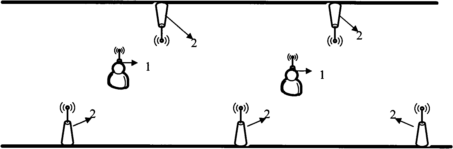
[0021] Embodiment 1: The coal mine underground wireless sensor network node equipment has a wireless sensor fixed node 1 and a wireless sensor mobile node 2, the fixed sensor node 1 is placed on the wall of the coal mine underground roadway, and one is placed at a certain distance, and the mobile sensor node 2 is worn on the On the underground personnel, it moves with the movement of the underground personnel.
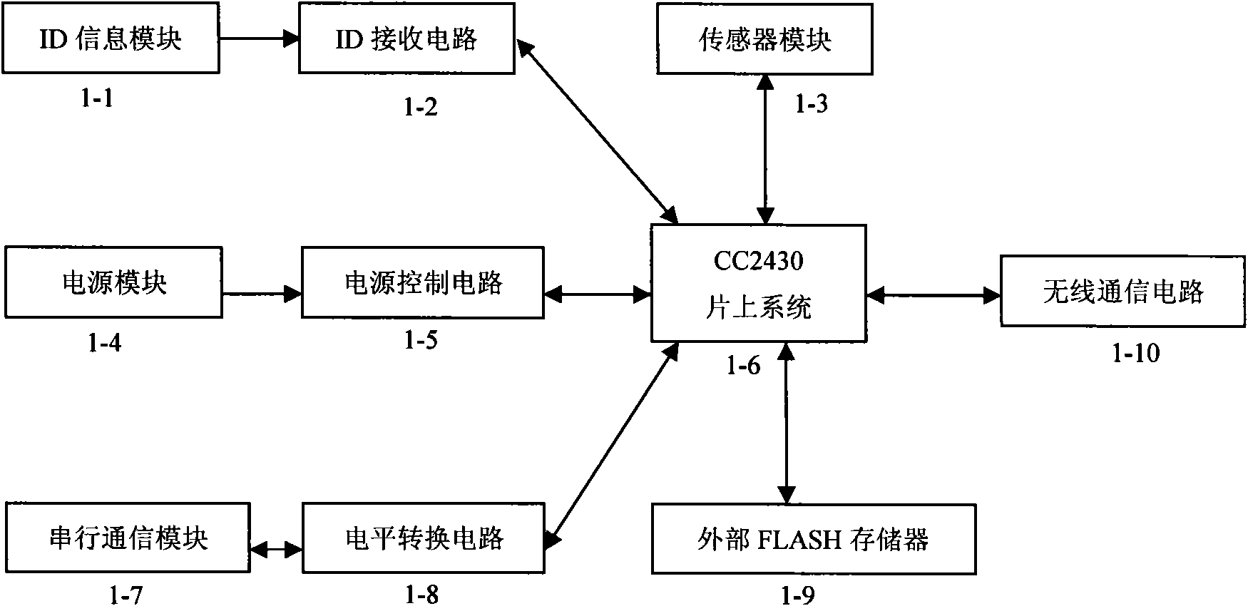
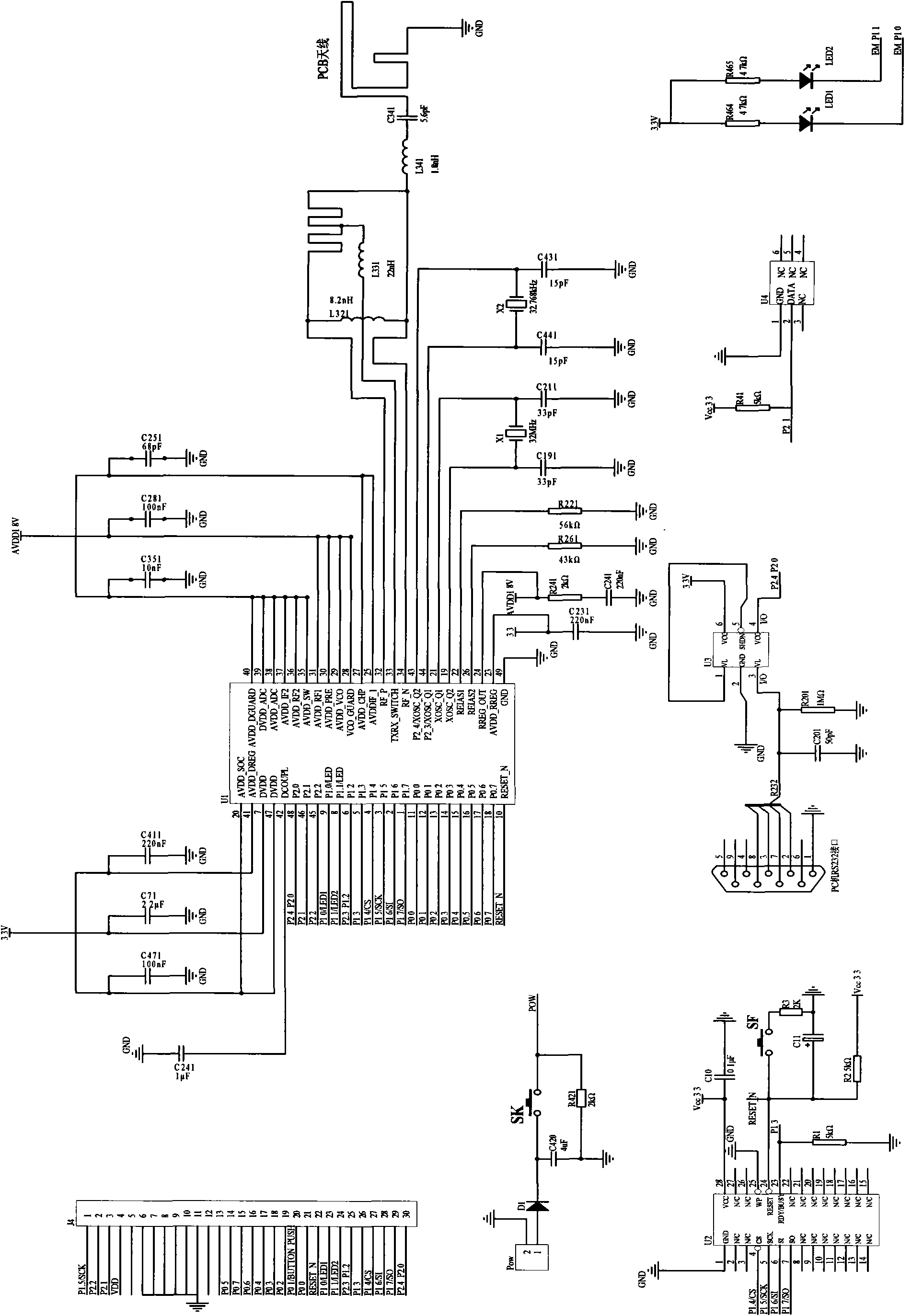
[0022] The wireless sensor fixed node 1 consists of a fixed ID information module 1-1, a fixed ID receiving circuit 1-2, a fixed sensor module 1-3, a fixed power supply module 1-4, a fixed power supply control circuit 1-5, and a fixed CC2430 on-chip System 1-6, fixed serial port communication module 1-7, fixed level conversion circuit 1-8, fixed external FLASH memory 1-9, fixed wireless communication circuit 1-10, fixed ID information module 1-1 receives through fixed ID The circuit 1-2 is connected with the fixed CC2430 SoC 1-6; the fixed power module 1-4 is connected with the fixed CC2430 SoC 1-6 through the fixed power control circuit 1-5; the fixed serial port communication module 1-7 is converted through the fixed level The circuit 1-8 is connected to the fixed CC2430 SoC 1-6; the fixed sensor module 1-3, the fixed external FLASH memory 1-9 and the fixed wireless communication circuit 1-10 are all connected to the fixed CC2430 SoC 1-6.
[0023] The wireless sensor mobile node 2 is composed of a mobile ID information module 2-1, a mobile ID receiving circuit 2-2, a mobile power supply module 2-3, a mobile power supply control circuit 2-4, a mobile CC2430 system on chip 2-5, and a mobile serial port Composed of communication module 2-6, mobile level conversion circuit 2-7, and mobile wireless communication circuit 2-8, mobile ID information module 2-1 is connected with mobile CC2430 system-on-chip 2-5 through mobile ID receiving circuit 2-2; The power module 2-3 is connected with the mobile CC2430 system-on-chip 2-5 through the mobile power supply control circuit 2-4; the mobile serial port communication module 2-6 is connected with the mobile CC2430 system-on-chip 2-5 through the mobile level conversion circuit 2-7; The wireless communication circuit 2-8 is connected with the mobile CC2430 SoC 2-5.
[0024] The fixed power supply control circuit 1-5 and the mobile power supply control circuit 2-4 of the wireless sensor fixed node and the wireless sensor mobile node have a DC-DC control circuit and an intrinsically safe power supply protection circuit, and the DC-DC control circuit is connected to the intrinsically safe power supply protection circuit. connect.
[0025]The DC-DC control circuit includes the integrated circuit U5. Pin 1 of the integrated circuit is connected to the battery through a resistor, and pin 1 is also grounded through a resistor. Pins 2, 3, 4, 5, 8, and 9 are all connected through a resistor or capacitor. Ground, pin 6 is grounded, pin 7 is connected to the gate of the field effect tube, the source and drain of the field effect tube are grounded at one end, and one end is connected to the battery through an inductance, and pin 10 is connected to the 9 Pin and pin 3 are connected, and pin 9 is the output terminal.
[0026] The intrinsically safe power supply protection circuit is composed of a current monitoring chip, a Zener tube, a triode, a diode, a capacitor and a resistor. There is a voltage divider at one end, the midpoint of the voltage divider is connected to the control electrode of the thyristor, the cathode of the thyristor is connected to the bases of the transistor VT5 and the transistor VT3 through a diode, and the collector of the transistor VT5 is connected to the base of the transistor VT4 Connection, the collector of the triode VT4 is the output terminal, the emitter of the triode VT4 is connected to the output terminal of the current monitoring chip in series, and the 3 pins of the current monitoring chip connected in series are connected to the base of the triode VT2; both pins are grounded, The transistor VT2 is connected to the base of the transistor VT3 through a resistor, and the collector of the transistor VT3 is connected to the base of the transistor VT2 through a resistor and a diode.
[0027] Both the fixed power supply control circuit 1-5 and the mobile power supply control circuit 2-4 of the wireless sensor fixed node and wireless sensor mobile node are provided with 5V voltage by dry batteries, and the voltage is sent to the DC-DC control circuit composed of LTC1871 chip through the POW5V port. The circuit continuously and constantly controls the output voltage so that the output voltage is the standard voltage 3.3V required by the present invention. The voltage is sent out from the Vout3.3V port, connected to the Vin3.3V port, and the standard voltage is sent to the current monitoring chip ZXCT1010, voltage regulator ZR431L, four FMMT491 triodes, two diodes and several capacitors in series. In the intrinsically safe power supply protection circuit composed of resistors, overcurrent and overvoltage protection is carried out to meet the requirements of intrinsic safety. Finally, the stable and safe 3.3V voltage is supplied to the entire node through the Vcc3.3V terminal. The switching circuit is connected with the capacitor C420, the resistor R421 and the diode D1, in order to reduce the instantaneous energy generated during operation, thus forming an intrinsically safe circuit.
[0028] exist figure 1 Among them, it is characterized in that the intrinsically safe wireless sensor network system in coal mine consists of fixed wireless sensor node 1 and wireless sensor mobile node 2. The fixed sensor nodes 1 are placed on the wall of the coal mine underground roadway, one at a certain distance, and the mobile sensor nodes 2 are placed on the underground personnel and move with the movement of the underground personnel.
[0029] exist figure 2 Among them, when the wireless communication circuit 1-10 receives the wireless signal of the wireless sensor mobile node 2, the signal is driven through the wireless data interface of the CC2430 system-on-chip 1-6 to drive the internal crystal oscillator to wake up the wireless sensor fixed node 1, and the ID information module 1- 1 Receive the ID signal sent by the wireless sensor mobile node through the ID information receiving circuit 1-2 connected to it, and transmit it to the CC2430 system on chip 1-6, and the CC2430 system on chip 1-6 processes the internal data The identity and location information are sent out via the internal wireless data interface 1-6 of the CC2430 SoC and the external wireless communication circuit 1-10, and then transmitted to the ground monitoring center through multi-hop between fixed wireless sensor nodes. The sensor module 1-3 transmits the collected gas concentration, temperature and humidity signals to the CC2430 SoC 1-6. The CC2430 SoC 1-6 converts the analog signal into a digital signal through the internal A/D converter, and saves the data in the internal memory and the external FLASH memory 1-9. The energy of the entire node is provided by the power supply module 1-4, and the required voltage is provided to the node through the adjustment of the power supply control circuit 1-5. Serial communication modules 1-7, level conversion circuits 1-8, and CC2430 system-on-chip 1-6 are connected in series to realize communication between fixed wireless sensor nodes and other external devices.
[0030] exist image 3 , the list of chips in the figure:
[0031] U1: CC2430 system on chip, CC2430 chip can realize data receiving, processing and transmitting functions.
[0032] U2: AT45DB041, external memory.
[0033] U3: MAX3371, used to implement bidirectional level conversion of TTL and RS-232.
[0034] U4: DS2401, ID generator.
[0035] J4: Expansion slot for CC2430 chip.
[0036] CC2430 SoC is the core part of the whole node equipment, which includes a series of functions such as data reception, processing and transmission. Because the I/O interface of the CC2430 chip is limited, it needs to be expanded, and the "14-19" end of the J4 expansion slot is connected to the external sensor module. External FLASH memory U2, its function is to save the data collected by the node, so that the data will not be lost when the wireless sensor fixed node suddenly loses power. Since U1 and U2 use low-level reset, in the reset circuit of the system, the 24th pin of U2 connected to them and the 10th pin of U1 are reversed, which realizes that when the switch operates in the reset circuit, Realize the low level reset of U1 and U2. The 4th pin is the chip selection signal of U2, and the 5th pin is the serial clock signal of U2, which is used to control the read and write operations of data.
[0037] In order to burn the internal program of the wireless sensor fixed node, the wireless sensor fixed node realizes the two-way communication between U1 and the computer. Because U1 adopts TTL level, and the serial interface of PC is mostly RS-232 level, the two levels are different and cannot be directly connected, and an external interface is required for level matching. The wireless sensor fixed node uses the U3 chip to realize the two-way level conversion of TTL and RS-232. Pin 4 of U3 is connected to pin 48 of U1 to realize bidirectional data transmission. U4 is an ID signal generator, used to identify the identity of underground personnel. Pin 2 of U4 is connected to pin 46 of U1 to transmit data to U1.
[0038] Two LED signal indicators are used to display the working status of the wireless sensor fixed node. LED1 reflects the working status of node signal reception and transmission. After the node is woken up, it enters the working mode to receive and send data. In this mode, U1 controls LED1 through pin 9 to make it blink at a frequency of 1 time per second. LED2 reflects whether the wireless sensor fixed node is in a normal state. After the wireless sensor fixed node is powered on, U1 controls LED2 through the 8th pin to make it flash once every five seconds. In this way, only the state of the wireless sensor fixed nodes can be known, and the energy consumption is reduced.
[0039] exist Figure 4 Among them, U2 needs to be reset before storing data. This function can be realized by installing the reset switch after the fixed node of the wireless sensor is powered on. U2 uses a low-level reset, so the 24th pin of U2 is inverted. When triggered, the reset function is not implemented, and the pin is usually at a high level. C11 and R2 are RC circuits designed to prevent the switch from generating sparks in the contact mode, so that it can meet the requirements of intrinsic safety. The 4th pin is the chip selection signal terminal of U2, U2 is enabled through 4 pins, and reads and writes data through serial output and serial input. When the chip select signal is pulled low, pull the 5-pin serial clock signal terminal, control the operation code and buffer address, and input it through the 6-pin serial input terminal; when all the data is loaded, under the control of the 5-pin serial clock, the master The data in the stored page can be read out from the 7-pin serial output. The 23-pin U1 is connected to the 5-pin, and the U2 is sent to U1 whether it is in a busy state, that is, whether it is storing data.
[0040] exist Figure 5 Among them, after the mobile node 2 enters the working mode, the ID information is generated by the ID information module 2-1, and is sent to the CC2430 system-on-chip 2-5 through the ID sending circuit 2-2 connected thereto, and the CC2430 system-on-chip 2-5 passes through After the internal data processing, the ID information and the information of the mobile node are sent to the fixed node 1 through the wireless communication circuit 2-8. The energy of the mobile node is provided by the power supply module 2-3, and the required voltage is provided to the node through the adjustment of the power control circuit 2-4. The serial communication module 2-6, the level conversion circuit 2-7, and the CC2430 SoC 2-5 are connected in series to realize the communication between the wireless sensor mobile node and other external devices.
[0041] exist Image 6 Among them, U1 is the core part of the node, which can perform a series of functions such as data reception, processing, and transmission. Since U1 is a low-level reset, it realizes its low-level reset requirement through an external reset switch circuit. U4 is an ID signal generator for identification of personnel. Pin 2 of U4 is connected to pin 46 of U1 to transmit data to U1. In order to burn the internal program of the wireless sensor mobile node, the wireless sensor mobile node realizes the two-way communication between U1 and the computer. Because U1 adopts TTL level, and the serial interface of PC is mostly RS-232 level, the two levels are different and cannot be directly connected, and an external interface is required for level matching. The wireless sensor fixed node uses the U3 chip to realize the two-way level conversion of TTL and RS-232. Pin 4 of U3 is connected to pin 48 of U1 to realize bidirectional data transmission.
[0042] SK in the figure is a switch of the power supply. When the switch is set to 1, the power supply supplies power to the mobile node, making it enter the working mode. When set to 0, the node stops working. In order to meet the requirements of intrinsic safety, an RC circuit is connected to reduce the instantaneous energy generated during operation.