

Method for manufacturing printed wiring board
A technology for printed wiring boards and manufacturing methods, which is applied in the manufacturing of printed circuits, printed circuits, multilayer circuits, etc., can solve problems such as difficult waste liquid treatment, and achieve the effect of easy waste liquid treatment and removal of stains.
Inactive Publication Date: 2010-03-03
MEC CO LTD
View PDF6 Cites 4 Cited by
- Summary
- Abstract
- Description
- Claims
- Application Information
AI Technical Summary
Problems solved by technology
[0018] However, the potassium permanganate used in the decontamination process has a high possibility of
Method used
View moreImage
Smart ImageViewing Examples

Examples
Example Embodiment
[0101] [Example]
Login to View More PUM
 Abstract
The present invention relates to a method for manufacturing printed wiring board, which can easily process waste liquid and can fully obtain the stain spot removing effect. The method for manufacturing printed wiring board, in a method for manufacturing the printed wiring board irradiating laser on a multi-layer laminated board formed by a resin layer and a copper layer and forming with hole, comprises: a swelling process working procedure for dipping the multi-layer laminated board irradiated by laser in a non-oxidative swelling agent; a microetching process working procedure for leading a microetching to contact with the multi-layer laminated board after the swelling process working procedure; and an ultrasonic wave process working procedure for externally adding ultrasonic wave under the state of the multi-layer laminated board dipped in solution after the swelling process working procedure. The method for manufacturing the printed wiring board of the present invention can easily process waste liquid because the oxidative resin solvent such as potassium permanganate solution, and the like, are not used, but use the non-oxidative swelling agent; and the stain spot remained in the hole can be removed by the swelling process, the microetching process and the ultrasonic wave process.
Description
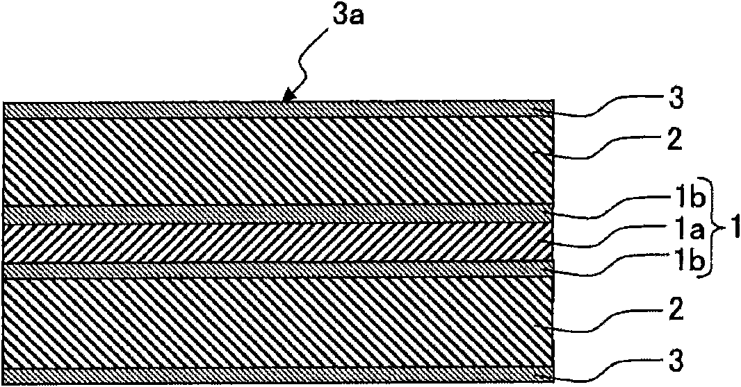
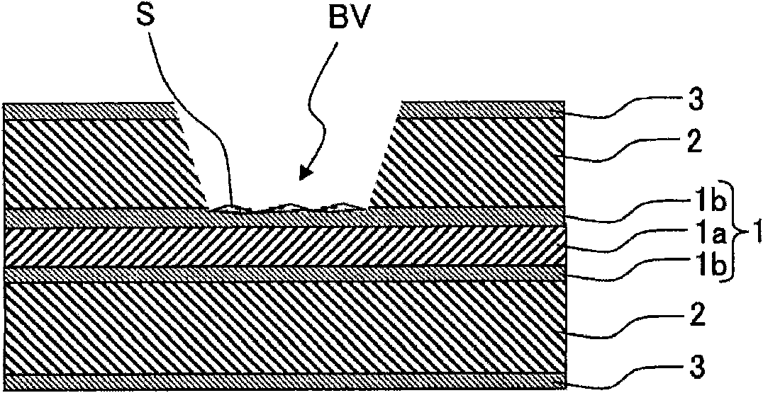
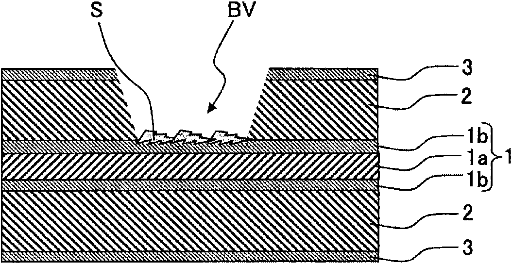
technical field [0001] 【0001】 [0002] The present invention relates to a method of manufacturing a printed wiring board in which holes are formed by irradiating laser beams on a multilayer laminated resin layer and copper layer. Background technique [0003] 【0002】 [0004] Due to miniaturization, higher density and higher functionality of electronic devices in recent years, printed wiring boards are also required to form high-density circuits. In order to meet this requirement, layer-to-layer connections are performed in multilayer printed wiring boards, and holes such as blind vias as bottomed holes and through-hole vias as through holes are formed. As a method of opening holes at this time, laser processing such as a carbon dioxide laser is often used in consideration of processing efficiency and cost. [0005] 【0003】 [0006] Taking a conformal mask as an example, a conventional method of forming holes by laser processing will be described with reference to the draw...
Claims
Login to View More Application Information
Patent Timeline
 IPC IPC(8): H05K3/46H05K3/00H05K3/26H05K3/42
CPCH05K3/40
Inventor中村幸子池尻笃泰
OwnerMEC CO LTD