

Production method of low-surface-reflectivity diamond wire-cut polycrystalline silicon wafer texture
A technology of diamond wire cutting and polycrystalline silicon wafers, which is applied in the field of solar energy applications, can solve the problems of mechanical damage on the surface of silicon wafers, high reflectivity, expensive equipment, etc., and achieve the effects of industrial production, simple waste liquid treatment, and long lifetime of few carriers
- Summary
- Abstract
- Description
- Claims
- Application Information
AI Technical Summary
Problems solved by technology
Method used
Image

Examples
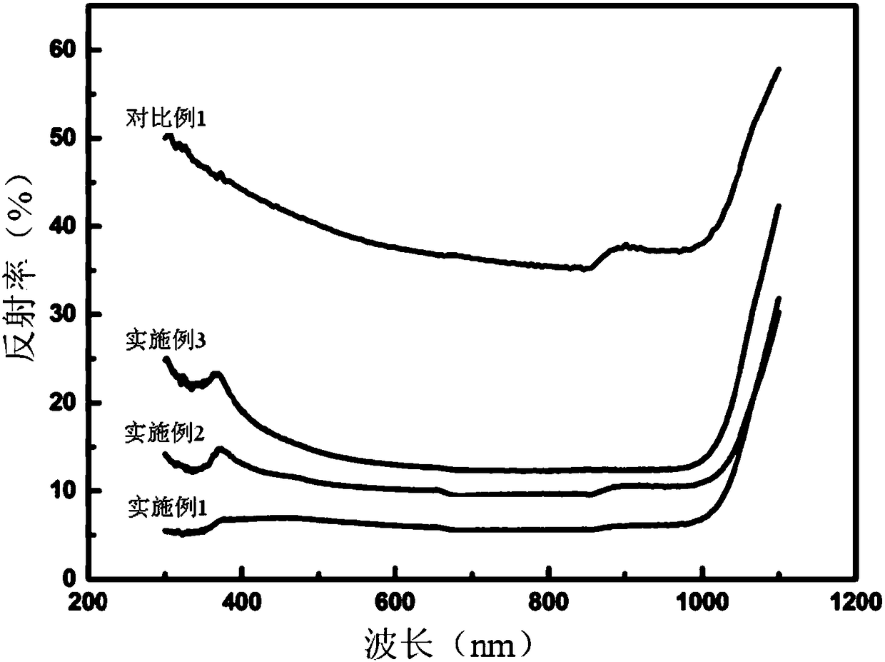
Embodiment 1
[0046] (1) Put a diamond wire-cut polycrystalline silicon wafer with a thickness of 180±5 μm and a size of 30mm×30mm into ethanol for ultrasonic cleaning, and then put it into an RCA solution for cleaning at 80°C to remove organic matter and metal ions on the surface of the silicon wafer;
[0047] (2) Put the cleaned silicon wafer into a polytetrafluoroethylene reaction kettle filled with corrosive liquid, seal it, and react for 30 minutes at 30°C. The corrosive liquid is HF, Fe(NO 3 ) 3 and ethanol mixed aqueous solution, the concentration of HF in the mixed solution is 10mol / L, Fe(NO 3 ) 3 The concentration of ethanol is 0.2mol / L, and the volume percent concentration of ethanol is 1%. A porous structure is formed on the surface of the silicon wafer after etching;
[0048] (3) Put the silicon chip obtained in step 2 into an alkaline mixed solution for reaction. The alkaline mixed solution is formed by mixing ammonia water with a concentration of 25% by mass, hydrogen pero...
Embodiment 2
[0051] (1) Put a diamond wire-cut polycrystalline silicon wafer with a thickness of 180±5 μm and a size of 30mm×30mm into ethanol for ultrasonic cleaning, and then put it into an RCA solution for cleaning at 80°C to remove organic matter and metal ions on the surface of the silicon wafer;
[0052] (2) Put the cleaned silicon wafer into a polytetrafluoroethylene reactor filled with corrosive liquid, seal it, and react for 40 minutes at 30°C. The corrosive liquid is HF, Fe(NO 3 ) 3 and ethanol mixed aqueous solution, the concentration of HF in the mixed solution is 10mol / L, Fe(NO 3 ) 3 The concentration of ethanol is 0.4mol / L, and the volume percent concentration of ethanol is 1%. A porous structure is formed on the surface of the silicon wafer after etching;
[0053] (3) Put the silicon chip obtained in step 2 into an alkaline mixed solution for reaction. The alkaline mixed solution is formed by mixing ammonia water with a concentration of 25% by mass, hydrogen peroxide wit...
Embodiment 3
[0058] (1) Put a diamond wire-cut polycrystalline silicon wafer with a thickness of 180±5 μm and a size of 30mm×30mm into ethanol for ultrasonic cleaning, and then put it into an RCA solution for cleaning at 80°C to remove organic matter and metal ions on the surface of the silicon wafer;
[0059] (2) Put the cleaned silicon wafer into a polytetrafluoroethylene reaction kettle filled with corrosive liquid, seal it, and react at 30°C for 60 minutes. The corrosive liquid is HF, Fe(NO 3 ) 3 and ethanol mixed aqueous solution, the concentration of HF in the mixed solution is 5mol / L, Fe(NO 3 ) 3 The concentration of ethanol is 0.2mol / L, and the volume percent concentration of ethanol is 1%. A porous structure is formed on the surface of the silicon wafer after etching;
[0060] (3) Put the silicon chip obtained in step 2 into an alkaline mixed solution for reaction. The alkaline mixed solution is formed by mixing ammonia water with a concentration of 25% by mass, hydrogen perox...
PUM
| Property | Measurement | Unit |
|---|---|---|
| Life expectancy | aaaaa | aaaaa |
| Life expectancy | aaaaa | aaaaa |
| Life expectancy | aaaaa | aaaaa |
Abstract
Description
Claims
Application Information