Testing of electronic circuits using an active probe integrated circuit

A technology of integrated circuits and probes, used in electronic circuit testing, measurement leads/probes, components of electrical measuring instruments, etc., to achieve the effect of improving performance and high-frequency signal integrity

Inactive Publication Date: 2010-03-24
SCANIMETRICS
View PDF2 Cites 18 Cited by
  • Summary
  • Abstract
  • Description
  • Claims
  • Application Information

AI Technical Summary

Problems solved by technology

These circuits are implemented on a PCB located on a load board for testing packaged parts, not on a semiconductor device for testing a device in wafer form, and thus the problem of signal transmission and degradation through the PCB remains

Method used


Image

  • Testing of electronic circuits using an active probe integrated circuit
  • Testing of electronic circuits using an active probe integrated circuit
  • Testing of electronic circuits using an active probe integrated circuit

Examples


Embodiment Construction

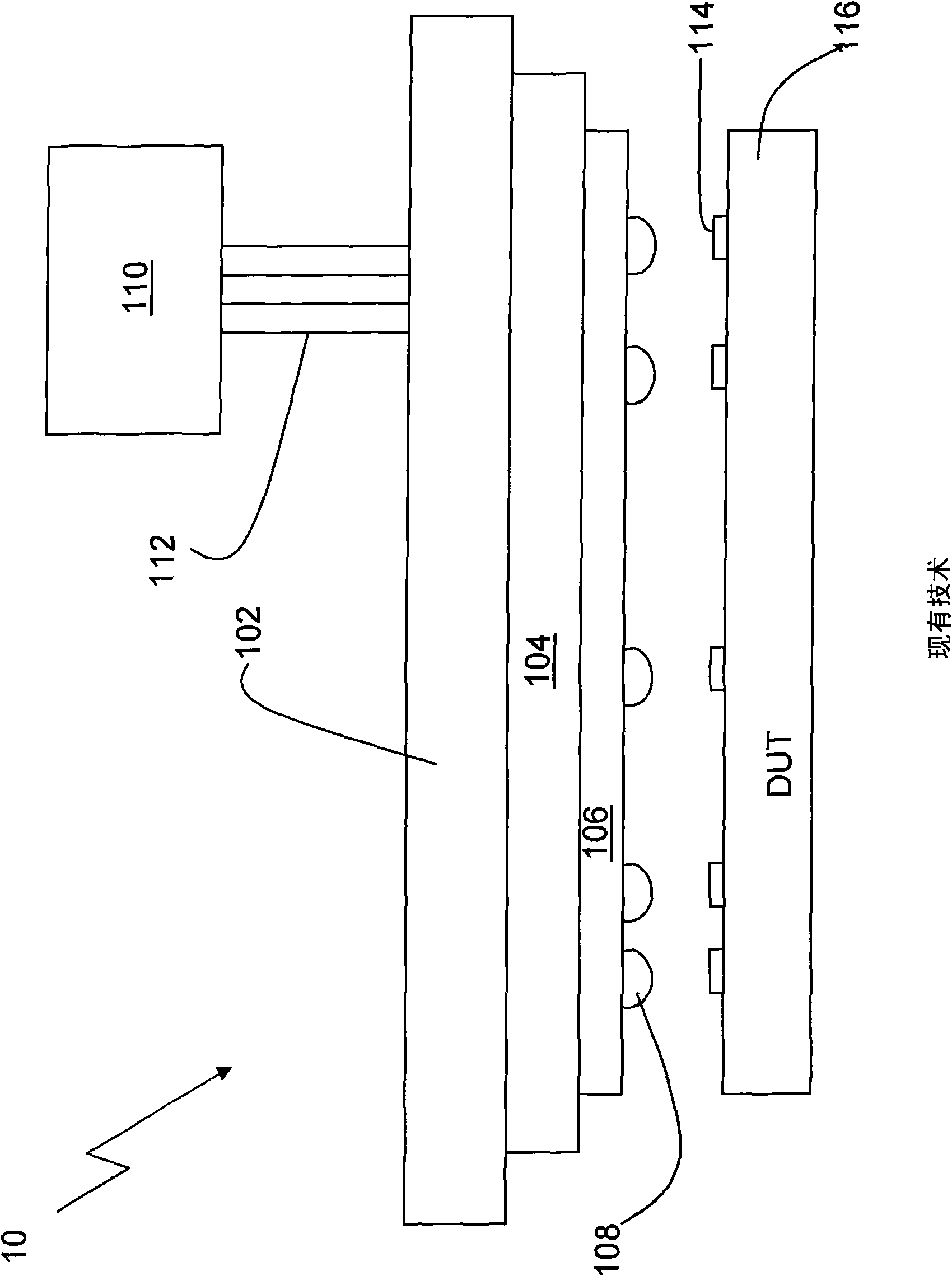
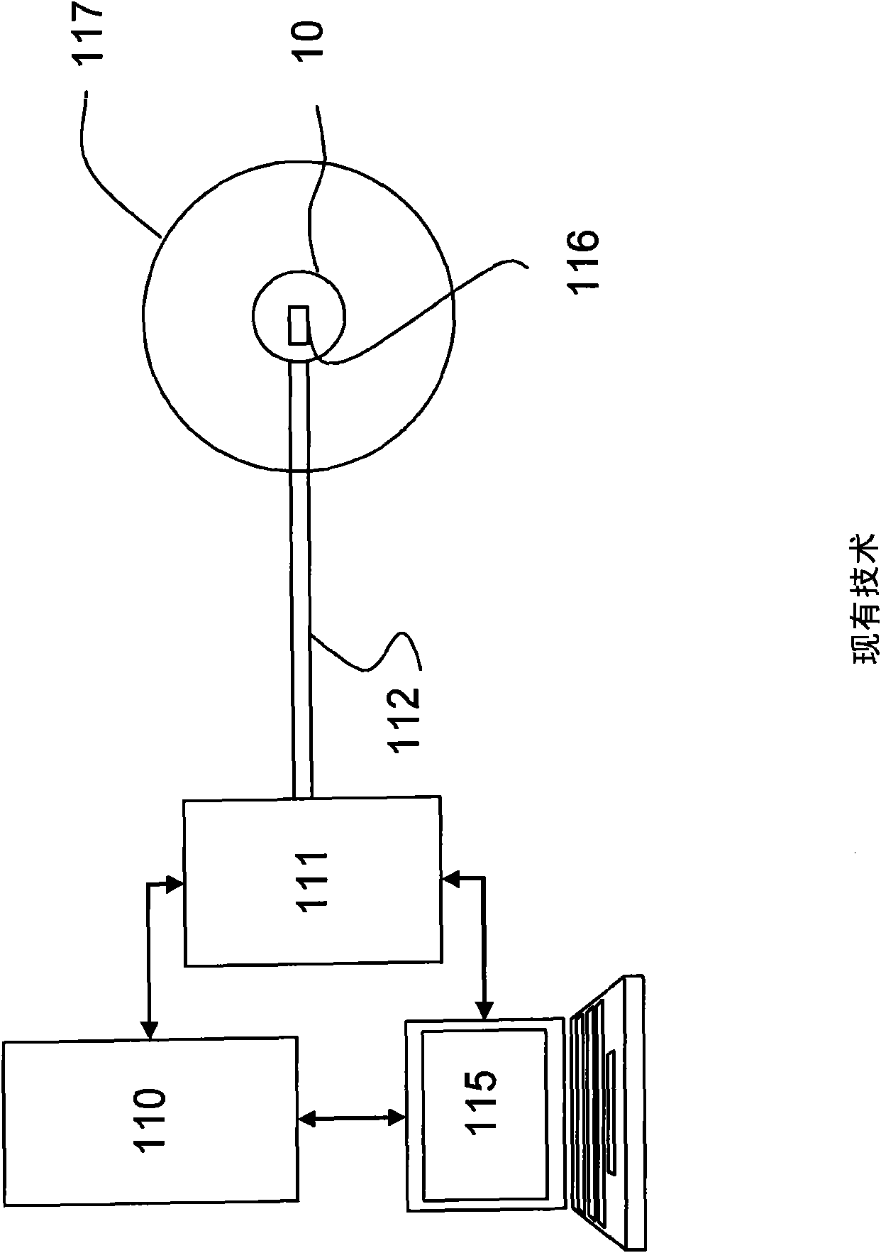
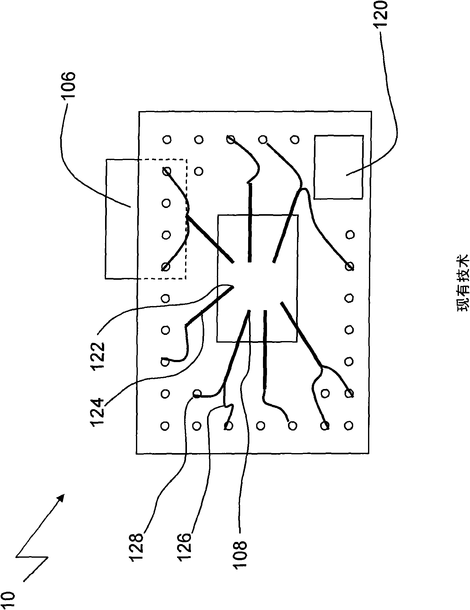
[0072] The following description relates to a novel probe card structure for testing electronic devices, especially integrated circuits (ICs). The concept is called an "active probe".

[0073] The principles of the described apparatus and method are applicable to probe testing and thus can test several types of ICs, including but not limited to ICs such as RF, serializer / deserializer (SerDes), memory, logic, parametric, digital ICs for signal processing as well as applications in logic circuits and digital devices. The processes and apparatus described here are illustrated using as an example a probe card with active probes for RF wafer testing using RF as the high frequency signal. Those of ordinary skill in the art will appreciate that the principles can be applied to several other applications, such as testing high-speed digital circuits, networking circuits, microprocessors, high-frequency circuits, high-precision analog memory devices, and mixed signal circuits. example...


PUM


Abstract

A method and apparatus are provided for transmission/reception of signals between automatic test equipment (ATE) and a device under test (DUT). A probe card has a plurality of associated proximate active probe integrated circuits (APIC) connected to a plurality of probes. Each APIC interfaces with one or more test interface points on the DUT through probes. Each APIC receives and processes signalscommunicated between the ATE and the DUT. Low information content signals transmitted from the ATE are processed into high information content signals for transmission to the probe immediately adjacent the APIC, and high information content or time critical signals received by the APIC from the DUT are transmitted as low information content signals to the ATE. Because the APIC is immediately adjacent the probe there is minimum loss or distortion of the information in the signal from the DUT.

Description

technical field [0001] The present invention relates to apparatus and methods for testing electronic circuits using active probe integrated circuits. Background technique [0002] As integrated circuit (IC) devices have become more and more complex, the cost of test has gradually risen to the point where both the technical limitations of the industry and the cost of test are of concern. As a result, efforts are continuing to reduce the overall cost of test equipment. These motivations are further reinforced by the continued drive to reduce component costs. Thus, removing any wasted overhead from testing and packaging has gained significant attention in recent years and will continue to play an important role. Industry and market data show that the operation and maintenance of test equipment accounts for a major portion of the total cost of test. [0003] Currently existing and proposed solutions have technical limitations. Typically, integrated circuits (ie, devices unde...

Claims


Application Information

Patent Timeline
Patent Type & Authority Applications(China)
IPC IPC(8): G01R1/067G01R1/30G01R1/07G01R31/3185
CPCG01R31/318505G01R31/31905G01R1/07385G01R31/3025G01R1/07342G01R1/067G01R31/28G01R31/3185G01R1/06711G01R1/06722G01R1/06727G01R1/07307
Inventor S·斯卢普斯凯B·莫尔C·V·塞拉塔蒙比
Owner SCANIMETRICS
Why Eureka
Try Eureka