Substrate cleaning device

A technology for cleaning devices and substrates, used in grinding machines, metal processing equipment, grinding/polishing equipment, etc., which can solve the problems of rapid wear of cleaning blades, frequent replacement, and poor cleaning ability.

Inactive Publication Date: 2010-05-12
AU OPTRONICS (SUZHOU) CORP LTD +1
View PDF0 Cites 11 Cited by
  • Summary
  • Abstract
  • Description
  • Claims
  • Application Information

AI Technical Summary

Problems solved by technology

[0004] The conventional method is to use a scraper with a certain pressure to scrape off the residue on the surface of the panel. However, the scraping effect of the scraper is limited, and in the scraping method in the prior art, the pressure applied to the scraper is fixed. With cushioning effect, it is easy

Method used


Image

  • Substrate cleaning device
  • Substrate cleaning device
  • Substrate cleaning device

Examples


Embodiment Construction

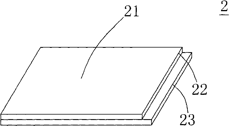
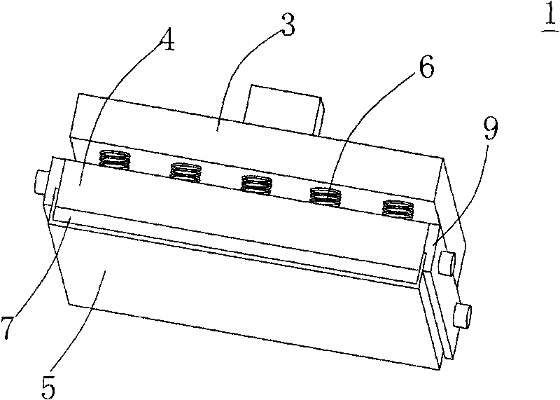
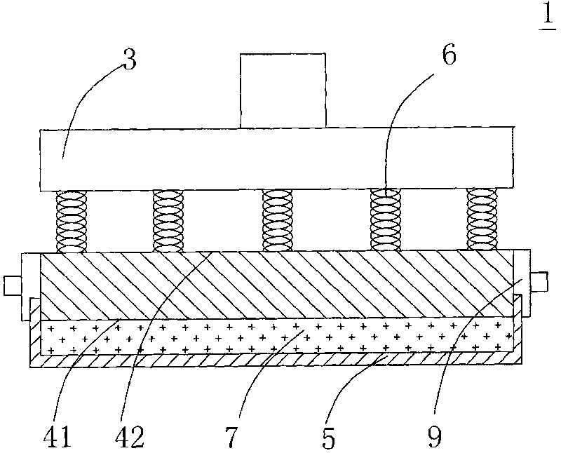
[0021] See figure 1 , figure 2 and image 3 , figure 1 Shown is a schematic diagram of a liquid crystal display panel, figure 2 Shown is a schematic perspective view of the cleaning device according to the present invention, image 3 shown as figure 2 Front view of the cleaning unit in . The substrate cleaning device 1 provided by the present invention is used to remove foreign matter on the surface 21 of a substrate 2, wherein the substrate 2 is, for example, glass or a display panel. In this embodiment, the substrate 2 is taken as an example of a liquid crystal display panel, the liquid crystal display panel 2 includes a color filter substrate 22 and a TFT array substrate 23 , and the surface 21 is located on the side of the color filter substrate 22 as an example. In the field of liquid crystal displays, in the manufacturing process of the liquid crystal display panel 2, before attaching the polarizer, the panel will be cleaned first. Glue or foreign matter will c...


PUM


Abstract

The invention provides a substrate cleaning device for cleaning foreign matters on the surface of a substrate. The cleaning device comprises a cleaning pressure head, a base, a grinding belt and a pressure buffering unit. The cleaning pressure head provides pressure for the substrate. The base is arranged relative to the cleaning pressure head and is provided with a first surface and a second surface which are opposite to each other, and the first surface is far away from the cleaning pressure head. The grinding belt is arranged on the first surface of the base, fixed on the base and used for grinding the surface of the base. The pressure buffering unit is arranged between the cleaning pressure head and the base and connected with the cleaning pressure head and the base. The cleaning device utilizes the grinding belt to clean the surface of the substrate instead of a scraper, thereby effectively improving the cleaning capability of equipment, lowering the replacing frequency of the grinding belt and reducing the damage probability of the substrate.

Description

technical field [0001] The invention relates to a cleaning device, in particular to a cleaning device for removing foreign matters on the surface of a glass substrate. Background technique [0002] The production and manufacturing of liquid crystal displays can be mainly divided into: array process, panel process and module process. Among them, the array process is mainly to form a large number of transistors on the glass substrate through similar semiconductor manufacturing techniques (coating, exposure, development, etching, etc.) on the glass substrate. The panel process is mainly to combine the glass substrate manufactured by the array process with the glass substrate of the color filter, and pour liquid crystal between the two sealed glass substrates. Finally, the panel module production is mainly to assemble the cut panel with external components such as driver IC, circuit board, polarizer and backlight components. [0003] In the panel manufacturing process, when tw...

Claims


Application Information

Patent Timeline
IPC IPC(8): B24B21/04B24B21/18
Inventor 周盼华孙玮夏仁贤张良
Owner AU OPTRONICS (SUZHOU) CORP LTD
Why Eureka
Try Eureka