Encapsulating structure of semiconductor chip and manufacturing technology thereof

A technology of packaging structure and manufacturing process, which is applied in the direction of semiconductor/solid-state device manufacturing, semiconductor devices, semiconductor/solid-state device components, etc. It can solve the problems that the welding protective coating cannot fully penetrate, and the protective layer cannot effectively cover the lead metal layer. , to achieve the effect of ensuring electrical performance, improving quality and enhancing stability

Active Publication Date: 2010-05-19
CHINA WAFER LEVEL CSP
View PDF0 Cites 16 Cited by
  • Summary
  • Abstract
  • Description
  • Claims
  • Application Information

AI Technical Summary

Problems solved by technology

[0010] On the other hand, in the above-mentioned wafer-level chip size packaging process, since the welding protective coating is directly applied after the UBM layer is formed by electroplating, the soldering protective coating cannot fully penetrate into the center of the dicing line of the adjacent chip, so the After the adjacent chip is cut along the center of the dicing line, the protective layer 218 cannot effectively cover the end surface b on the side wall of the package on the lead metal layer 214, which eventually leads to figure 1 The generation of defects at A in

Method used


Image

  • Encapsulating structure of semiconductor chip and manufacturing technology thereof
  • Encapsulating structure of semiconductor chip and manufacturing technology thereof
  • Encapsulating structure of semiconductor chip and manufacturing technology thereof

Examples


Embodiment

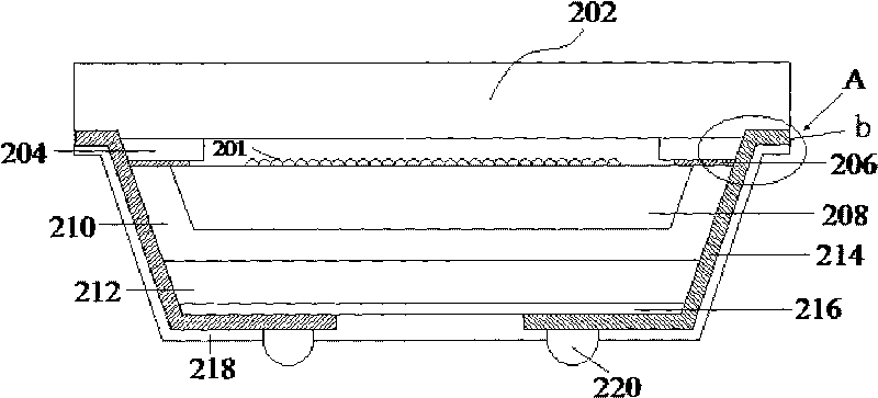
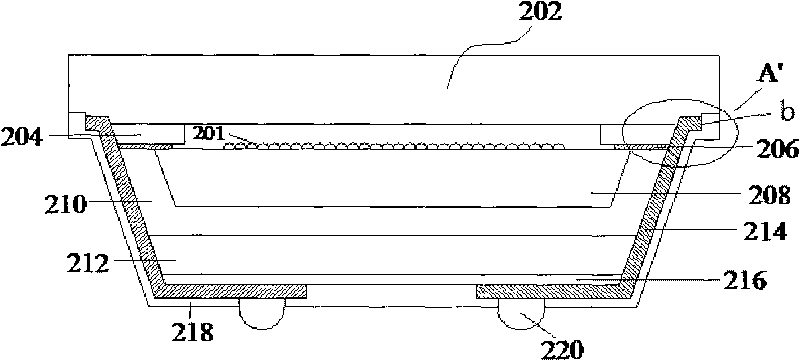
[0043] Example: first combine figure 2 As shown, the semiconductor chip packaging structure provided by the present invention is a wafer-level chip-scale packaging structure, which includes a package body, a chip 208 packaged in the package body and containing a photosensitive element 201, and a solder pad connected to the chip 208 206. The lead metal layer 214 connected to the exposed side of the solder pad 206 in a T-shaped connection and extending along the side wall of the package to the back of the package and connected to the solder bump 220, and the protection covering the outer surface of the lead metal layer 214 Layer 218. The package described in this embodiment is specifically composed of a substrate 202, a cavity wall 204 arranged on the substrate 202 in a closed-loop structure, a resin layer 210, an insulating layer 216, and a glass layer 212. The front side of the chip 208 passes through the solder pad 206. The cavity wall 204 on the substrate 202 is pressed to...


PUM


Abstract

The invention provides an encapsulating structure of a semiconductor chip, comprising an encapsulating body, a chip, a weld pad, a leading wire metal layer and a protecting layer, wherein, the chip is encapsulated into the encapsulating body and comprises a photosensitive element; the weld pad is connected with the chip; the leading wire metal layer is connected with the exposed part of the side surface of the weld pad in a T-shaped connection mode, extends to the back of the encapsulating body from the side wall of the encapsulating body and is connected with a welding bulge; and the protecting layer covers the outer surface of the leading wire metal layer. The encapsulating structure is characterized in that the protecting layer is also used for coating the end surface of the side wall of the encapsulating body on the leading wire metal layer. The encapsulating structure strengthens the stability of a connecting point of the welding side surface and the leading wire metal layer in the encapsulating structure of the semiconductor chip, ensures the electrical property of the connecting point and further improves the quality of a semiconductor chip encapsulating product.

Description

technical field [0001] The invention relates to a packaging structure of a semiconductor chip and a manufacturing process thereof. Background technique [0002] At present, the wafer-level chip size packaging technology in the field of semiconductor chip packaging technology mainly leads the pads 206 on the chip 208 to the back of the package through the way of side electrode extraction, which is different from traditional packages such as ceramic leadless chip carriers (Ceramic) Leadless Chip Carrier), Organic Leadless Chip Carrier (Organic Leadless Chip Carrier) and digital camera modular money-making methods, the lead-out structure is as follows figure 1 As shown in A, the exposed side of the solder pad 206 is connected to the lead metal layer 214 in a T-shaped connection, and the lead metal layer 214 further extends from the side wall of the package of the chip 208 to its back and is connected to the solder bump 202. And the outer surface of the lead metal layer 214 is ...

Claims


Application Information

Patent Timeline
Patent Type & Authority Applications(China)
IPC IPC(8): H01L23/482H01L23/488H01L21/50H01L21/60H01L21/78
CPCH01L2224/13
Inventor 王之奇邹秋红俞国庆王蔚
Owner CHINA WAFER LEVEL CSP
Why Eureka
Try Eureka