Layout structure for promoting pixel defection detectivity of thin film transistor substrate

A thin-film transistor and layout structure technology, which is applied in the field of thin-film transistor substrate layout structure, can solve the problems of labor cost and GCshort did not propose a solution, and achieve the effect of saving labor cost

Active Publication Date: 2011-05-18
CENTURY DISPLAY (SHENZHEN) CO LTD
View PDF0 Cites 0 Cited by
  • Summary
  • Abstract
  • Description
  • Claims
  • Application Information

AI Technical Summary

Problems solved by technology

The current method is to locate the place where the lowest voltage appears on the "one" line, and start to find the short circuit with human eyes, which consumes labor costs
The existing technology does not propose an effective solution to GC short

Method used


Image

  • Layout structure for promoting pixel defection detectivity of thin film transistor substrate
  • Layout structure for promoting pixel defection detectivity of thin film transistor substrate
  • Layout structure for promoting pixel defection detectivity of thin film transistor substrate

Examples


Embodiment Construction

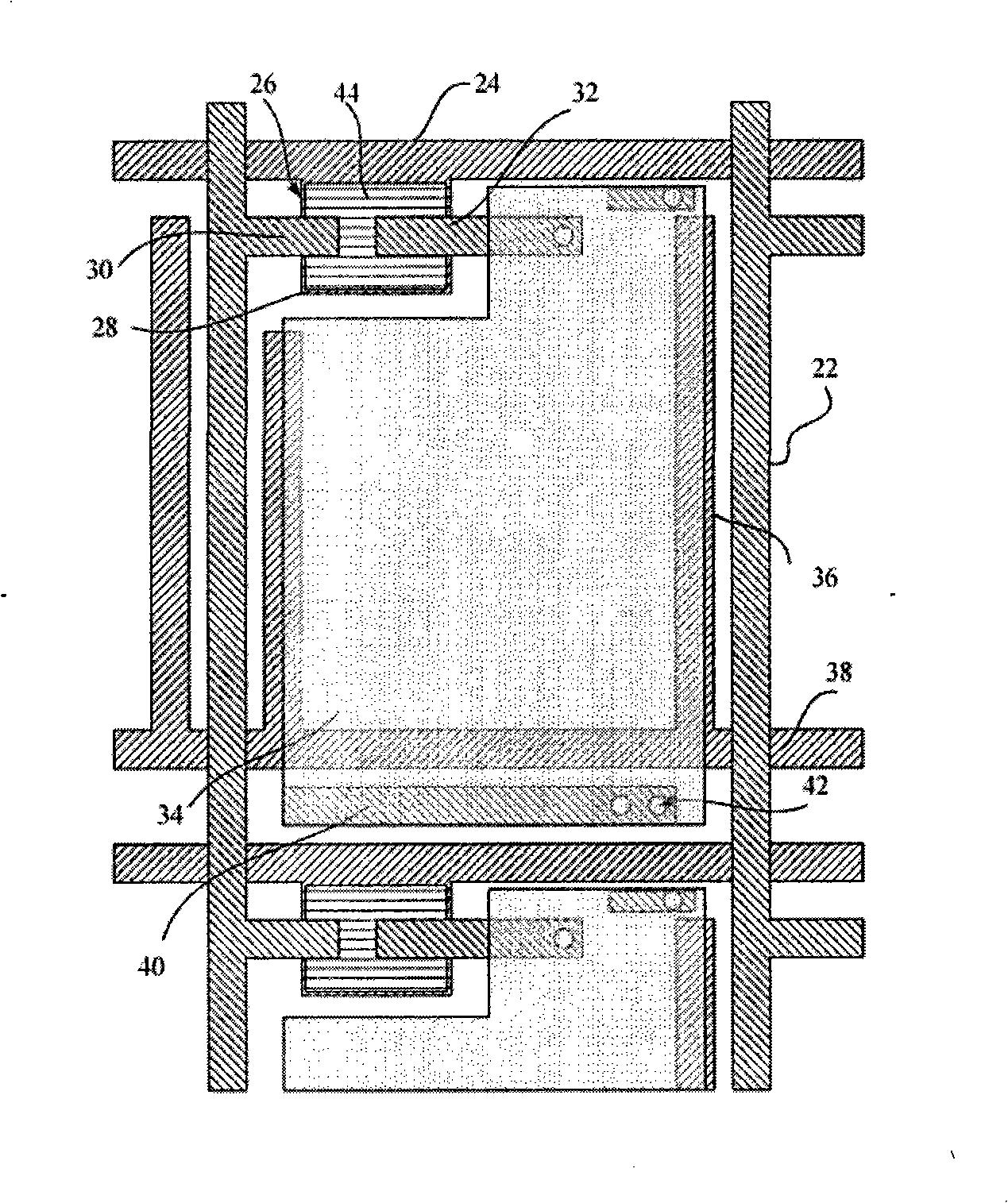
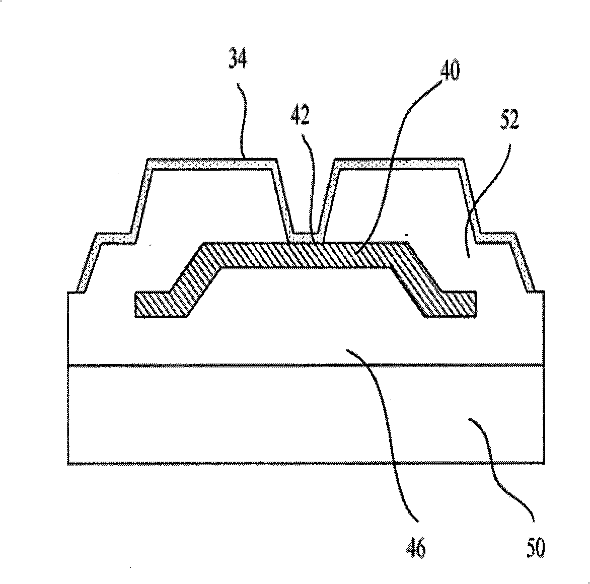
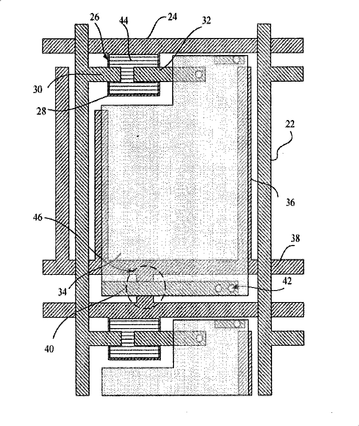
[0014] In order to describe in detail the layout structure of the present invention to improve the pixel defect detection rate of the thin film transistor substrate, please refer to figure 1 and figure 2 . figure 1 It is a layout structure for improving the pixel defect detection rate of the thin film transistor substrate of the present invention. The layout structure of the pixel defect detection rate of the TFT substrate of the present invention includes multiple columns of first data lines 22 and multiple rows of first scanning lines 24 . A plurality of columns of first data lines 22 and a plurality of rows of first scanning lines 24 define a plurality of pixels, and a thin film transistor 26 is formed in each pixel, and the thin film transistor 26 is used as a switch component, wherein a first metal The gate 28 of the thin film transistor 26, the first scanning line 24 and the common electrode wiring 38 are formed simultaneously; the drain 32, the source 30 and the firs...


PUM


Abstract

The invention provides a layout structure for promoting pixel defection detectivity of a thin film transistor substrate, comprising multiseriate first data lines and multi-row first scanning lines; a plurality of pixels are defined by utilizing the multiseriate first data lines and the multi-row first scanning lines; a thin film transistor is formed in each pixel; a gate electrode, the first scanning lines and a common electrode line of the thin film transistor are simultaneously formed by utilizing a first metal layer; a drain electrode, a source electrode and a first data line of the thin film transistor are formed on the thin film transistor by utilizing the second metal layer; the drain electrode of the thin film transistor is connected with a pixel electrode; the common electrode line is arranged adjacent to the first scanning line and the first data line, and is partially covered by the pixel electrode; a virtual data line is positioned between the first scanning line and the common electrode line, and is connected with the pixel electrode, can effectively and rapidly position short circuit of the GC short, and effectively solves the trouble having to be found by human eyes in the prior art.

Description

【Technical field】 [0001] The invention relates to a layout structure for improving the pixel defect detection rate of a thin film transistor substrate, in particular to a thin film transistor substrate layout structure for locating short-circuit defects by using dummy data lines. 【Background technique】 [0002] After the array process (Array process) is completed, an array process test (Array test) is equipped to check whether the thin film transistor meets the requirements. For example, in the Array test, it is checked whether the metal lines (scanning lines, data lines, common electrode wiring) meet the requirements, whether the transistors meet the requirements, and so on. [0003] When the test voltage is input, if there is a short circuit between the data line and the scanning line (source / gate line short, SG short), the screen of the detector will display a "cross" word line, and the intersection point of the cross is the short circuit (defect) , the positioning is ve...

Claims


Application Information

Patent Timeline
Patent Type & Authority Patents(China)
IPC IPC(8): H01L23/528G01R31/28
Inventor 余鸿志
Owner CENTURY DISPLAY (SHENZHEN) CO LTD
Why Eureka
Try Eureka