COG chip inversion bonding device

A bonding device and chip technology, applied in electrical components, semiconductor/solid-state device manufacturing, circuits, etc., can solve problems such as unstable chip position, low chip accuracy, and impact on bonding position accuracy.

Inactive Publication Date: 2010-05-26
SUNEAST ELECTRONICS TECH SHENZHEN +1
View PDF0 Cites 9 Cited by
  • Summary
  • Abstract
  • Description
  • Claims
  • Application Information

AI Technical Summary

Problems solved by technology

When the existing chip is taken out, because the position in the chip magazine is not fixed, that is, the position and direction of multiple chips are not unique, so when the chip is taken out, the direction and position of each chip are different. At the same time, the position of the chip is not fixed, which affects the accuracy of the bonding position; at the same time, when the chip

Method used


Image

  • COG chip inversion bonding device
  • COG chip inversion bonding device
  • COG chip inversion bonding device

Examples


Embodiment Construction

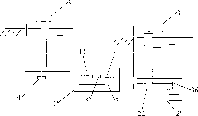
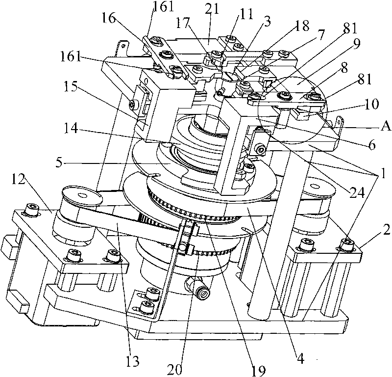
[0031] like figure 1 As shown, the present invention provides an embodiment of a COG chip flip-chip bonding device.

[0032] The COG chip flip-chip bonding device includes: a pre-calibration clamping device 1' for correcting the position of the chip, a substrate positioning device 2' for positioning the glass substrate bonded with the chip, and transporting the chip and A conveying device 3' for glass substrates, wherein the pre-calibrated clamping device 1' and the substrate positioning device 2' are fixed on the base in sequence, and the conveying device 3' is connected with the pre-calibrated clamping device 1' respectively It is connected with the driving part on the substrate positioning device 2'.

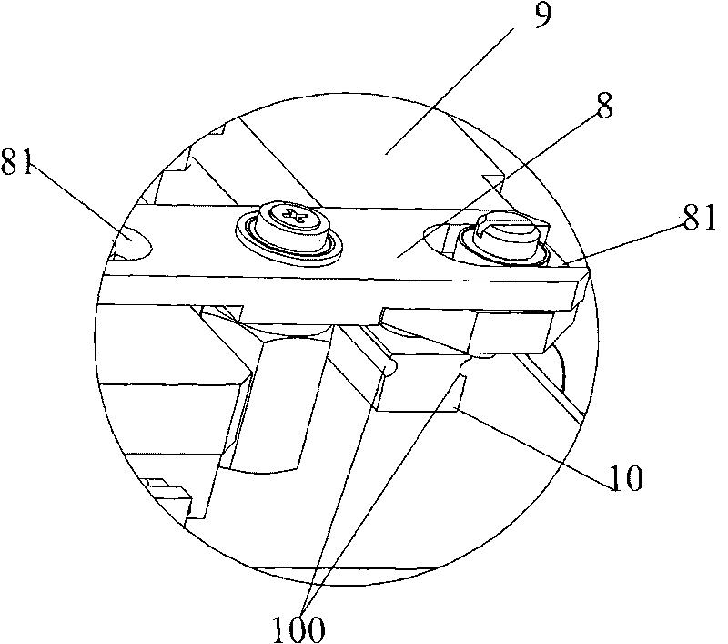
[0033] The chip 4' is transported to the fixing device 3 on the pre-calibration clamping device 1' by the conveying device 3', and is corrected in the same aspect by the first calibration block 7 and the second calibration block 11 The glass substrate 36 for bonding is tran...


PUM


Abstract

The invention discloses a COG chip inversion bonding device which comprises a precalibration clamping device, a base plate positioning device and a delivering device, wherein the precalibration clamping device calibrates the position of a chip; the base plate positioning device positions a glass base plate bonded with the chip; the delivering device delivers the chip and the glass base plate; the precalibration clamping device and the base plate positioning device are sequentially fixed on a base; and the delivering device is respectively connected with drive parts on the precalibration clamping device and the base plate positioning device. The traditional delivering device chip is placed in the position of the precalibration clamping device, and the precalibration clamping device chip carries out precalibration; the position of the glass base plate on the base plate positioning device is calibrated by the base plate positioning device; and finally, the control device controls the clamping device to bond the chip on the glass base plate. Because the positions of the chip and the glass base plate are respectively calibrated before the chip is bonded, the bonding precision of the chip can be improved.

Description

technical field [0001] The invention relates to a COG chip flip-chip bonding device for the COG chip bonding process on a glass display substrate. Background technique [0002] COG uses anisotropic conductive film ACF and thermocompression welding technology to mount the integrated circuit chip on the glass substrate of the display screen, thereby reducing the product volume, increasing the assembly density, reducing costs, and realizing large-scale production. COG technology is widely used in various flat-panel displays and personal mobile products, and is currently the highest packaging form of packaging. [0003] During the COG chip bonding process, various means and methods must be used to take the chip out of the material box and transfer it to the bonding position on the glass plate to achieve precise positioning with the glass plate. [0004] In the existing COG chip bonding process, it is necessary to take out the bonded chip from the material box and transfer it to...

Claims


Application Information

Patent Timeline
IPC IPC(8): H01L21/00H01L21/50H01L21/68
Inventor 区大公张志能孔繁松李克天陈新度欧阳祥波
Owner SUNEAST ELECTRONICS TECH SHENZHEN
Why Eureka
Try Eureka