Electrostatic discharge protection semiconductor device and method for mafacturing the same

A semiconductor and conductive technology, applied in the field of electrostatic discharge protection semiconductor devices and their manufacturing, can solve problems such as loss interface

Inactive Publication Date: 2010-05-26
DONGBU HITEK CO LTD
View PDF2 Cites 5 Cited by
  • Summary
  • Abstract
  • Description
  • Claims
  • Application Information

AI Technical Summary

Problems solved by technology

Also, the electrons and holes ionized by impacts in the lower edge gate region 111 may deplete the interf

Method used


Image

  • Electrostatic discharge protection semiconductor device and method for mafacturing the same
  • Electrostatic discharge protection semiconductor device and method for mafacturing the same
  • Electrostatic discharge protection semiconductor device and method for mafacturing the same

Examples


Embodiment Construction

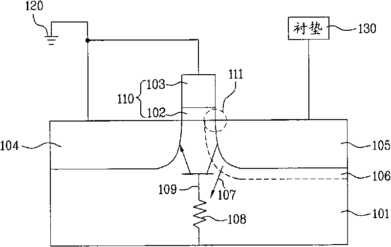
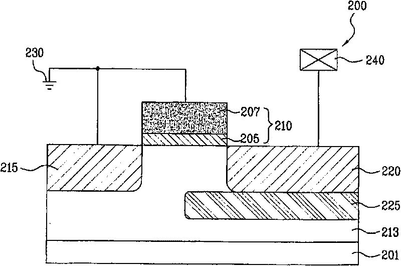
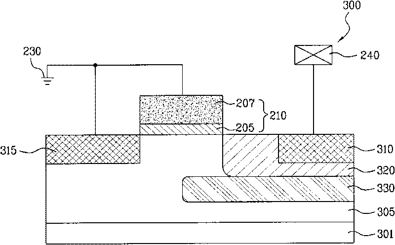
[0027] The embodiment of the present invention relates to an electrostatic discharge protection semiconductor device. reference example figure 2, the ESD protection semiconductor device 200 may include a gate 210 , a source region 215 , a first drain region 220 and a second drain region 225 . According to an embodiment of the present invention, the gate 210 may include a gate oxide layer 205 and a gate electrode 207 , and may be multi-layered in and / or over the substrate 201 . In an embodiment of the present invention, the source region 215 may be formed in and / or over a predetermined region of the substrate 201 on one side of the gate 210 . In an embodiment of the present invention, the first drain region 220 may be formed in and / or over a predetermined region of the substrate 201 on the side opposite to the gate 210 .

[0028] According to an embodiment of the present invention, the second drain region 225 may be connected to a lower region of the first drain region 220 ....


PUM


Abstract

An electrical device, including a semiconductor device such an electrostatic discharge protection semiconductor device, and a method for manufacturing the same. An electrostatic discharge protection semiconductor device may include a substrate and a gate in and/or over the substrate. The gate may be multi-layered, and may include a gate oxide layer and a gate electrode. An electrostatic discharge protection semiconductor device may include a source region formed in and/or over a predetermined area of the substrate on a side of the gate, and a plurality of drain regions which may be sequentially multi-layered in and/or over the substrate on an opposing side of the gate in a vertical direction. At least one drain region may be overlapped with the gate in a horizontal direction.

Description

[0001] This application claims priority from Korean Patent Application No. 10-2008-0097104 (filed on October 2, 2008) based on 35 U.S.C119, the entire contents of which are hereby incorporated by reference. technical field [0002] The present invention relates to a semiconductor device, and more particularly, to an electrostatic discharge protection semiconductor device and a manufacturing method thereof, wherein the abnormal leakage current ( abnormal leakage current). Background technique [0003] Embodiments of the present invention relate to an electronic device. Some embodiments of the present invention relate to a semiconductor device (eg, an electrostatic discharge protection semiconductor device) and a method of manufacturing the same. [0004] Recently, semiconductor devices such as high voltage semiconductor devices have been widely developed and used in various applications including liquid crystal display (LCD), integrated circuit (IC), and other technologies. ...

Claims


Application Information

Patent Timeline
IPC IPC(8): H01L29/78H01L29/06H01L21/336H01L23/60
CPCH01L29/66659H01L29/1045H01L29/78H01L29/7835H01L29/0847H01L2924/0002H01L2924/00H01L27/04
Inventor 金锺玟宋宗圭金山弘
Owner DONGBU HITEK CO LTD
Why Eureka
Try Eureka