

Image sensor and manufacturing method thereof
An image sensor and substrate technology, applied in semiconductor/solid-state device manufacturing, image communication, electric solid-state devices, etc., can solve the problems of dark current reduction saturation and sensitivity, image error, output image sensitivity reduction, etc.
- Summary
- Abstract
- Description
- Claims
- Application Information
AI Technical Summary
Problems solved by technology
Method used
Image

Examples
Embodiment Construction
[0019] When the terms "on" or "over" are used herein and refer to a layer, region, pattern or structure, it needs to be understood that a layer, region, pattern or structure may be directly on another layer or structure, or that intervening layers, intervening layers, or structures may also be present. region, intermediate pattern, or intermediate structure. When the terms "under" or "beneath" are used herein and refer to a layer, region, pattern or structure, it is to be understood that a layer, region, pattern or structure may be directly beneath another layer or structure, or that intervening layers, intervening regions may also be present. , intermediate pattern or intermediate structure.
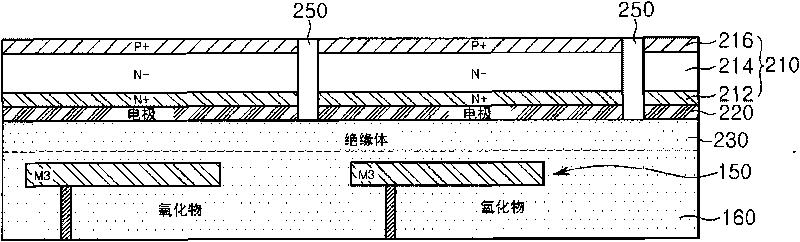
[0020] figure 1 It is a cross-sectional view showing an image sensor according to an embodiment of the present invention.
[0021] see figure 1 , in an embodiment, the image sensor may include: a readout circuit 120 (such as Figure 5B shown in); the metal line 150 disposed on the f...
PUM
 Abstract
Description
Claims
Application Information