Liquid crystal display panel and liquid crystal display

A liquid crystal display panel and liquid crystal layer technology, applied in the direction of instruments, nonlinear optics, optics, etc., can solve the problems of large edge distance difference, uneven cell thickness, and inability to eliminate uneven cell thickness, so as to improve uniformity, The effect of improving quality

Active Publication Date: 2010-06-09
TRULY SEMICON
View PDF0 Cites 9 Cited by
  • Summary
  • Abstract
  • Description
  • Claims
  • Application Information

AI Technical Summary

Problems solved by technology

[0006] In fact, for liquid crystal display panels similar to the above two structures, the existing frame glue and spacers cannot eliminate the phenomenon of uneven cell thickness, and the distance between each edge of the display area and the edge of the corresponding glass substrate is quite different. In the process of laminating the color filter substrate and the thin film transistor array substrate, the thickness of the box will be uneven, which will affect the quality of the display screen

Method used


Image

  • Liquid crystal display panel and liquid crystal display
  • Liquid crystal display panel and liquid crystal display
  • Liquid crystal display panel and liquid crystal display

Examples


Embodiment 1

[0040] Figure 4 It is a schematic diagram of a liquid crystal display panel in this embodiment, Figure 5 for Figure 4 The cross-sectional view along the E-E' direction.

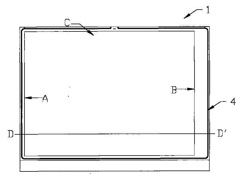
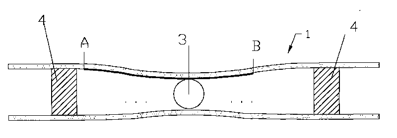
[0041] As shown in the figure, the liquid crystal display panel 10 includes: a first substrate 101, a second substrate 110, a liquid crystal layer (not shown in the figure) sandwiched between the two substrates, and a main bezel sealing the liquid crystal layer. 104 , the main frame glue 104 is basically arranged along the edge of the liquid crystal display panel 10 . In this embodiment, the liquid crystal display panel 10 is rectangular, and its display area C is also rectangular. Correspondingly, the main frame glue 104 is basically arranged along the rectangular edge of the liquid crystal display panel.

[0042] A plurality of spacers 103 are located in the display area C between the first substrate 101 and the second substrate 110 to maintain the distance between the two substrates. The first subst...

Embodiment 2

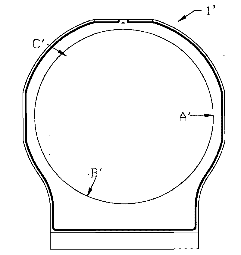
[0051] Image 6 It is a schematic diagram of the liquid crystal display panel in this embodiment. As shown in the figure, the liquid crystal display panel 20 is irregularly circular, including a circular area and a strip-shaped area integrated with the circular area. The display area of ​​the panel is circular, and its center is aligned with the liquid crystal display. The circular regions of the panels substantially coincide.

[0052] Same as the first embodiment, the main bezel glue 204 is basically arranged along the edge of the liquid crystal display panel 20 . However, in this embodiment, the liquid crystal display panel 20 is irregularly circular, and correspondingly, the main bezel glue 204 is basically also irregularly circular.

[0053] The main bezel 204 includes at least three subsections: a first subsection 204a, a second subsection 204b, and a third subsection 204c. The display area C of the liquid crystal display panel 20 includes at least three edges, wherein ...


PUM


Abstract

The invention provides a liquid crystal display panel and a liquid crystal display. The liquid crystal display panel comprises a first substrate, a second substrate, a liquid crystal layer between the two substrates and main frame glue sealing the liquid crystal layer, wherein the main frame glue is basically arranged along the edge of the liquid crystal display panel and at least comprises a first sub section and a second sub section. The liquid crystal display panel has a display area which at least comprises a first edge and a second edge, wherein the first edge corresponds to the first sub section of the main frame glue; the second edge corresponds to the second sub section of the main frame glue; the distance between the first edge and the first sub section is smaller than the distance between the second edge and the second sub section; and at least a section of auxiliary frame glue is arranged between the second edge and the second section. In liquid crystal display panel of the invention, under the condition of not influencing the characteristics of TFT-LCD, the auxiliary frame glue is added in a proper area in the two substrates to overcome the drawback of uneven box thickness and further improve the display effect of the liquid crystal display considerably.

Description

technical field [0001] The invention relates to the field of flat panel display technology, in particular to a liquid crystal display panel and a liquid crystal display. Background technique [0002] As a flat panel display, liquid crystal display (LCD) has many advantages such as clear and accurate image, thin thickness, light weight, no radiation, low energy consumption and low working voltage, and has been widely used in various fields. As the core component of the liquid crystal display, the liquid crystal display panel has two oppositely arranged substrates, and a liquid crystal layer arranged between the two substrates. The liquid crystal molecules in the liquid crystal layer are controlled by the electric field formed between the electrodes on the two substrates. deflection, and then adjust the transmittance of incident light to realize the control of bright and dark display pixels. [0003] At present, the driving of liquid crystal in thin film transistor liquid cry...

Claims


Application Information

Patent Timeline
Patent Type & Authority Applications(China)
IPC IPC(8): G02F1/1339
Inventor 胡君文李林廖从雄王磊谢凡何基强
Owner TRULY SEMICON
Why Eureka
Try Eureka