Liquid crystal display and driving method thereof
A technology of liquid crystal display and driving method, which is applied in the field of halftone technology, can solve the problems of reduced aperture ratio, increased power consumption, complex system circuit, etc., and achieve the effect of improving color shift phenomenon
- Summary
- Abstract
- Description
- Claims
- Application Information
AI Technical Summary
Problems solved by technology
Method used
Image

Examples
no. 1 example
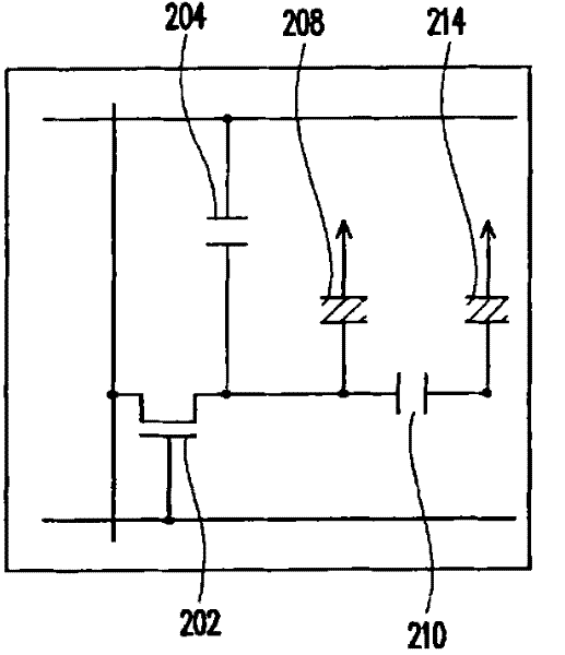
[0062] Figure 3A It is a pixel circuit diagram of the liquid crystal display according to the first embodiment of the present invention. The pixel 10 includes pixel capacitors 21 , 22 , transistors 31 , 32 and storage capacitors 41 , 42 . The second ends of the pixel capacitors 21 and 22 are coupled to the shared electrode, and the shared electrode is coupled to the common voltage V com . The first terminal, the second terminal and the gate terminal of the transistor 31 are respectively coupled to the first terminal of the pixel capacitor 21 , the data line DL and the scan line SL, and there is a parasitic capacitance 61 between the first terminal and the gate terminal of the transistor 31 . The first terminal, the second terminal and the gate terminal of the transistor 32 are respectively coupled to the first terminal of the pixel capacitor 22 , the data line DL and the scan line SL, and there is a parasitic capacitance 62 between the first terminal and the gate terminal o...
no. 2 example
[0084] Figure 5 It is a circuit diagram of a pixel of a liquid crystal display according to the second embodiment of the present invention. The pixel 11 of this embodiment is similar to the pixel 10 of the above-mentioned embodiment, and the components with the same numbers as those in FIG. 1 can refer to the above-mentioned embodiment. It should be noted that the pixel 11 in this embodiment also includes storage capacitors 43 and 44 . The first terminal and the second terminal of the storage capacitor 43 are respectively coupled to the first terminal and the second bias electrode of the transistor 31 . The first terminal and the second terminal of the storage capacitor 44 are respectively coupled to the first terminal and the second bias electrode of the transistor 32 . In this embodiment, the second bias electrode may be coupled to a ground voltage, for example. Therefore when modulating the common voltage V com When , the voltage across the pixel capacitor 21 ΔV P1 Th...
no. 3 example
[0092] Those skilled in the art can change the structure of the pixel according to requirements, for example Figure 7 It is a pixel circuit diagram of the liquid crystal display according to the third embodiment of the present invention. The pixel 12 of this embodiment is the same as the above-mentioned Figure 3A The pixel 10 is similar to that of the above-mentioned embodiments, and the components with the same numbers as those in the above-mentioned embodiments can refer to the above-mentioned embodiments. It should be noted that the sub-pixels 51 and 52 of this embodiment are respectively located on both sides of the data line DL, which has the advantage of reducing the complexity of the wiring. In addition, the pixel 12 also designs the storage capacitor 42 to be connected in parallel with the pixel capacitor 22 . Therefore, effects similar to those of the above-mentioned embodiments can also be achieved.
PUM
 Abstract
Description
Claims
Application Information