Silicon controlled rectifier and manufacturing method thereof

A silicon-controlled rectifier and doped region technology, applied in semiconductor/solid-state device manufacturing, electrical components, thyristors, etc., can solve the problems of difficult control of the trigger voltage value, increase the difficulty of the designer's design, etc., to reduce the design cost and ESD protection. The effect of improving the ability and reducing the trigger voltage value

Inactive Publication Date: 2010-06-09
HEJIAN TECH SUZHOU
View PDF0 Cites 32 Cited by
  • Summary
  • Abstract
  • Description
  • Claims
  • Application Information

AI Technical Summary

Problems solved by technology

However, these improved SCR structures have certain restrictions on reducing the trigger voltage, and the trigger voltage value is difficult to control, which increases the difficulty of the designer's design.

Method used


Image

  • Silicon controlled rectifier and manufacturing method thereof
  • Silicon controlled rectifier and manufacturing method thereof
  • Silicon controlled rectifier and manufacturing method thereof

Examples


Embodiment Construction

[0029] A silicon controlled rectifier according to the present invention will be further described in detail below in conjunction with the accompanying drawings and specific embodiments.

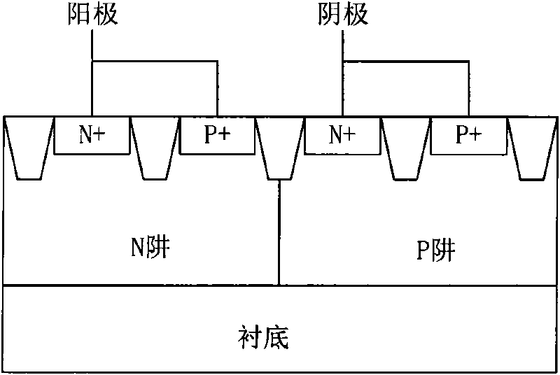
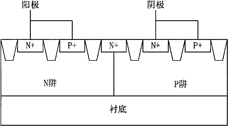
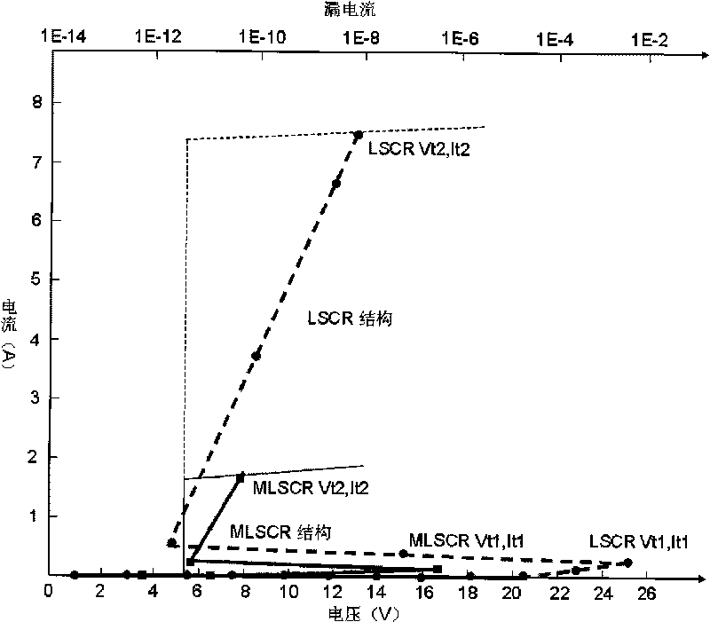
[0030] Such as figure 1 , 2 As shown in and 3, for example, the traditional lateral silicon-controlled rectifier LSCR structure and the improved lateral silicon-controlled rectifier MLSCR (Modified LSCR) in a certain process of 0.18 μm are taken as an example, because the traditional LSCR has a higher trigger voltage value, see image 3 In Vt1, the trigger voltage value is related to the breakdown voltage value of the N well Nwell / P well Pwell, and Vt1 is about 25V. Such a trigger voltage prevents the silicon controlled rectifier from being turned on in time during the ESD discharge process to effectively protect the internal The circuit cannot play a good role in protecting the device. At the same time, its secondary breakdown current value is about 7A, which is relatively high.

[0031...


PUM


Abstract

The invention discloses a silicon controlled rectifier and a manufacturing method thereof. The silicon controlled rectifier comprises a semiconductor substrate, a first P+ doped region, a first N+ doped region, a second P+ doped region, a second N+ doped region, a third P+ doped region or a third N+ doped region, a fourth P+ doped region or a fourth N+ doped region, wherein an N well and a P well are positioned above the semiconductor substrate; the first P+ doped region and the first N+ doped region are formed in the N well; the second P+ doped region and the second N+ doped region are formed in the P well; the third P+ doped region or the third N+ doped region is formed at the bonding position of the N well and the P well; and the fourth P+ doped region or the fourth N+ doped region is formed below the third P+ doped region or the third N+ doped region and in the N well or the P well. The invention has the advantages that the trigger voltage value of an SCR structure can be greatly decreased, thereby improving the integral protective capacity of an ESD; the trigger voltage value of a new SCR structure can be regulated according to the different requirements of a designer, so that the ESD can exert the optimal protective capacity in different circuit designs; and under the same ESD protection requirements, the area can be saved, thereby lowering the design cost.

Description

technical field [0001] The invention relates to a semiconductor device, in particular to a silicon controlled rectifier and a manufacturing method thereof. Background technique [0002] With the increasingly advanced semiconductor process, more and more designers pay more and more attention to the protection of electrostatic discharge (ESD) in IC design. The components that make up the ESD protection circuit include resistors (Resistor), diodes (Diode), triodes (Bipolar), gate grounded metal oxide half field effect transistors (GGMOSFET), gate coupled metal oxide half field effect transistors (GCMOSFET), silicon controlled rectifier (SCR), etc. [0003] Among many ESD protection devices, a silicon controlled rectifier (SCR) has the best ESD protection capability under the same area due to its lower holding voltage. However, when the SCR structure is used as an ESD protection device, it has a relatively high trigger voltage value (Vt1), so that the ESD protection effect of ...

Claims


Application Information

Patent Timeline
Patent Type & Authority Applications(China)
IPC IPC(8): H01L29/74H01L21/332
Inventor 石俊夏洪旭
Owner HEJIAN TECH SUZHOU
Why Eureka
Try Eureka