Process for encapsulating square flat outer-pin-free encapsulating structure

A technology of packaging structure and packaging technology, which is applied in the manufacture of electrical components, electrical solid devices, semiconductor/solid devices, etc., can solve problems such as process difficulties, burrs and bridging, design restrictions, etc., and achieve simple packaging technology, low cost, and avoid Glitches and the effect of pins bridging each other

Inactive Publication Date: 2010-06-16
SAMSUNG ELECTRONICS CO LTD +1
View PDF0 Cites 18 Cited by
  • Summary
  • Abstract
  • Description
  • Claims
  • Application Information

AI Technical Summary

Problems solved by technology

That is, when the spacing between inner pins decreases exponentially due to the increase of circuit density, it becomes more and more difficult to realize the separation of inner pins by cutting, and there will be many restrictions in terms of design
In particular, burrs and bridging are likely to occur when individual inner pins are separated by cutting

Method used


Image

  • Process for encapsulating square flat outer-pin-free encapsulating structure
  • Process for encapsulating square flat outer-pin-free encapsulating structure
  • Process for encapsulating square flat outer-pin-free encapsulating structure

Examples


Embodiment Construction

[0024] Hereinafter, the packaging process of the quadflat no-lead package structure according to the embodiment of the present invention will be described in detail with reference to the accompanying drawings. It should be noted that the drawings are not to scale and do not precisely reflect the precise structural or performance characteristics of any given embodiment, but are schematic only. In the drawings, the size and relative sizes of layers and regions are exaggerated for clarity.

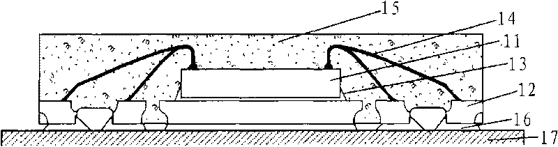
[0025] Figure 4 It is a schematic diagram showing the structure of the quadrilateral flat no outer lead package according to the present invention. Depend on Figure 4 It can be seen that the quadrilateral flat no-lead package structure according to the present invention comprises: a chip 41; a metal structure 42, on which the chip 41 is loaded at a predetermined position (die pad) on its upper surface; a metal wire 44, which is used to connect the chip The input / output port of 41 and the...


PUM


Abstract

The invention relates to a process for encapsulating a square flat outer-pin-free encapsulating structure. The encapsulating structure comprises a chip, a metal structure, a metal wire and a plastic encapsulating material; the encapsulating process comprises the following steps: manufacturing grooves with preset depth between adjacent inner pins and in connecting parts between the inner pins and other parts of the metal structure; adhering the chip to a preset position of the upper surface of the metal structure; connecting an input/output port of the chip with the inner pin which is positioned on the metal structure and corresponds to the input/output port through the metal wire; performing plastic encapsulation on the upper surface of the metal structure by the plastic packaging material so as to protect the chip, the metal wire and the upper surface of the metal structure; and thinning the metal structure upwards from the bottom plane of an encapsulating body with exposed metal after the plastic encapsulation so as to separate the adjacent inner pins and separate the inner pins from the other parts of the metal structure.

Description

technical field [0001] The invention relates to an electronic component packaging process, in particular to a packaging process of a square flat package structure without external leads, which makes pin arrangement more free and flexible, and can simplify the process. Background technique [0002] Package refers to connecting the input and output ports of the circuit on the chip to external joints or pins with metal wires, so as to connect with other devices or circuit boards. Package form refers to the housing used to install semiconductor integrated circuit chips. It not only plays the role of installing, fixing, sealing, protecting the chip and enhancing the electrothermal performance, but also connects the contacts on the chip to the pins of the package shell with metal wires, and these pins pass through the pins on the printed circuit board. The wires are connected with other devices, so as to realize the connection between the internal chip and the external circuit. ...

Claims


Application Information

Patent Timeline
Patent Type & Authority Applications(China)
IPC IPC(8): H01L21/50H01L21/60
CPCH01L2224/45124H01L2924/16195H01L2224/48091H01L2224/48247H01L2224/45147H01L2224/32245H01L2224/45139H01L2224/45144H01L2224/48465H01L2224/49433H01L2224/73265H01L2224/92247H01L2924/00014H01L2924/01015H01L2924/01047H01L2924/181H01L2924/00H01L2924/00012H01L2224/45015H01L2924/207
Inventor 梁乐
Owner SAMSUNG ELECTRONICS CO LTD
Why Eureka
Try Eureka