Electro-optical switch with low half-wave voltage

An electro-optic switch and half-wave voltage technology, applied in the field of optoelectronics, can solve the problem that the electro-optic crystal cannot be too long

Inactive Publication Date: 2010-06-23
FUJIAN CASTECH CRYSTALS
View PDF0 Cites 4 Cited by
  • Summary
  • Abstract
  • Description
  • Claims
  • Application Information

AI Technical Summary

Problems solved by technology

For some electro-optic crystals, the length of the electro-optic crystal itself is not long due to the growth reason or the volume of the laser is limited. To solve the problem of excessive wave voltage, the present invention provides a

Method used


Image

  • Electro-optical switch with low half-wave voltage
  • Electro-optical switch with low half-wave voltage
  • Electro-optical switch with low half-wave voltage

Examples


example 1

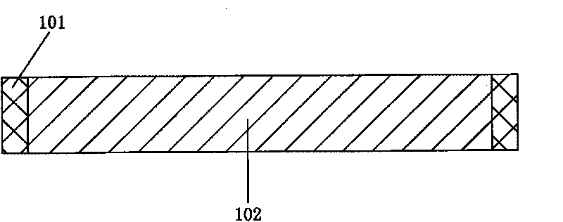
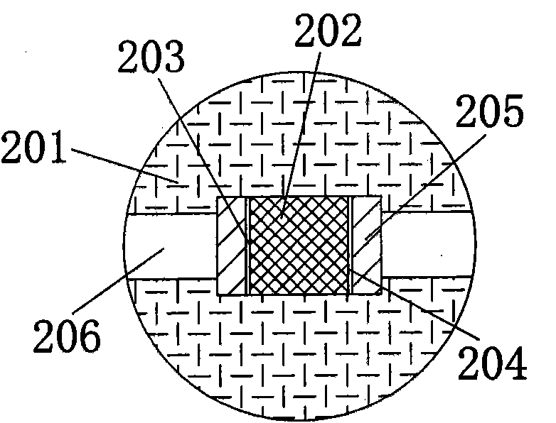
[0033] Example 1 The packaging implementation mode of the electro-optical switch of the present invention for single crystal or double crystal optical glue or glue or bond 1 see figure 1 , figure 2 and image 3 . The electro-optic switch in the figure includes a cylindrical insulating shell 201; there is a rectangular slot in the center of the shell, and an electro-optic crystal 202 is placed in the middle of the slot. The crystal can be BBO or LiNbO3 or LiTaO3 or RTA or RTP or KTP or LGS, etc., they It can be single crystal or double crystal photoresist or glued or bonded; a pair of sides of the crystal is plated with a metal conductive layer 203, and the length of the conductive layer is slightly shorter than the length of the crystal side; the metal conductive layer is attached with the same length or A slightly shorter indium foil 204; the indium foil is closely attached to the inner metal electrode 205 of the same length or slightly shorter; the outer metal electrode i...

example 2

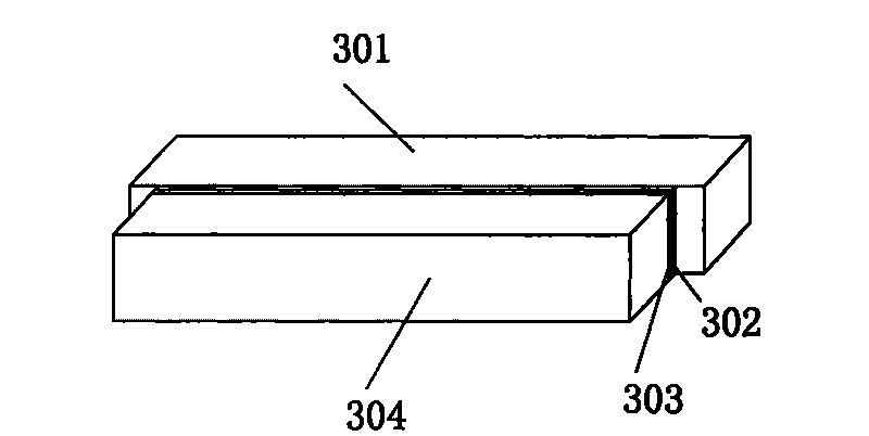
[0034] Example 2 For the packaging implementation mode 2 when the electro-optic switch of the present invention is used for double directly fixed crystals, see Figure 4 and Figure 5 . The electro-optic switch in the figure includes a cylindrical insulating shell 401; there is a rectangular slot in the center of the shell, and a pair of directly fixed electro-optic crystals 402 are placed in the middle of the slot, and they are arranged in series. The double crystals can be BBO or LiNbO3 or LiTaO3 or RTA or RTP or KTP or LGS, etc.; a metal conductive layer 403 is plated on a pair of sides of the crystal respectively, and the length of the conductive layer is slightly shorter than the length of the side of the crystal; the metal conductive layer is attached with an indium foil of the same length or slightly shorter 404; the indium foil is closely attached to an internal metal electrode 405 of the same length or slightly shorter than the indium foil; the internal metal electro...


PUM


Abstract

The invention discloses an electro-optical switch with low half-wave voltage, which comprises an insulating shell (201) and an electro-optic crystal (202); a pair of lateral surfaces of the crystal is plated with a metal conducting layer (203) respectively; an indium foil (204) is attached to the outside of the metal conducting layer; an inner metal electrode (205) is attached to the outside of the indium foil; and an external metal electrode hole (206) is reserved on the outside of the inner meal electrode. Through the electrode design, under the condition that the crystal has a certain length, when the electro-optical switch works, the ignition on the light-transmitting surface of the crystal caused by too close distance between the electrodes can be avoided so as not to influence the use of the switch or damage the light-transmitting surface of the crystal. The design effectively reduces the half-wave voltage of the electro-optical switch, prolongs the service life thereof and lowers the rigorous requirement on a switch driving power supply.

Description

technical field [0001] The invention relates to a pulse laser Q-switching device, which belongs to the field of optoelectronics, in particular to an electro-optic Q switch. technical background [0002] Electro-optic Q-switching refers to adding a polarizer and an electro-optic crystal in the laser cavity. After the light passes through the polarizer, it becomes linearly polarized light and reaches the electro-optic crystal. If a λ / 4 voltage is applied to the electro-optic crystal, due to the Pockels effect, the phase of the linearly polarized light will be delayed by π / 2 after passing through the electro-optic crystal once. The reflection of the cavity mirror changes the polarization direction of the linearly polarized light passing through the crystal by π / 2, so that the loss in the laser cavity is the largest, and the laser oscillation cannot be formed, reaching extinction. If no voltage is applied to the electro-optic crystal, the polarization direction of linearly pola...

Claims


Application Information

Patent Timeline
IPC IPC(8): G02F1/03H01S3/115
Inventor 江枫吴少凡庄松岩郑熠
Owner FUJIAN CASTECH CRYSTALS
Why Eureka
Try Eureka