

High-density printed circuit board (PCB) test machine and method
A testing method and testing machine technology, applied in the direction of measuring electricity, measuring devices, measuring electrical variables, etc., can solve problems such as increasing PCB packaging density, and achieve the effect of improving testing capabilities
- Summary
- Abstract
- Description
- Claims
- Application Information
AI Technical Summary
Problems solved by technology
Method used
Image

Examples
Embodiment Construction
[0041] The following describes in detail the implementation of XX of the present invention in conjunction with the accompanying drawings.
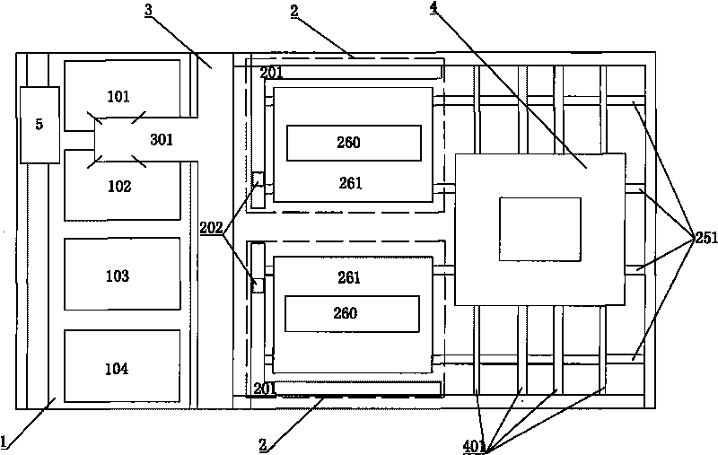
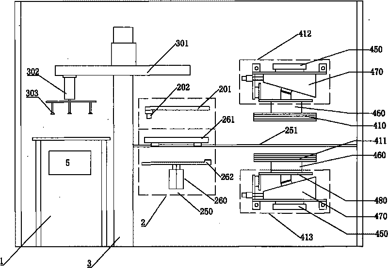
[0042] Such as figure 1 , 2 Shown, the present invention relates to a kind of high density PCB testing machine, it comprises:
[0043]Material table 1 includes four parts: the board to be tested placement area 101, the paper release area 102, the passed test board area 103, and the failed test board area 104. The setting of the material table 1 is used to load the PCB to be tested and provide good classification loading Good or bad PCB boards after testing.
[0044] There are PCB board clip sampling mechanisms 2 arranged side by side on the side of the material table 1, and usually in order to improve the use efficiency of the test fixture of the testing machine, at least two sets of clip sampling mechanisms 2 should be provided in the testing machine. In this embodiment, there are Two sets of independent snap-position alignment mechani...
PUM
 Abstract
Description
Claims
Application Information