Methods for Failure Analysis in Semiconductor Devices

A failure analysis and semiconductor technology, applied in the field of failure analysis, can solve problems such as primary failure analysis, achieve the effect of improving utilization rate, enhancing effect, and improving accuracy

Inactive Publication Date: 2015-10-14
SEMICON MFG INT (SHANGHAI) CORP +1
View PDF2 Cites 0 Cited by
  • Summary
  • Abstract
  • Description
  • Claims
  • Application Information

AI Technical Summary

Problems solved by technology

[0008] The problem solved by the present invention is to provide a method for failure analysis in semiconductor devices, and solve the problem in the prior art that only one failure analysis can be performed for the same semiconductor device

Method used


Image

  • Methods for Failure Analysis in Semiconductor Devices
  • Methods for Failure Analysis in Semiconductor Devices
  • Methods for Failure Analysis in Semiconductor Devices

Examples


Embodiment Construction

[0023] The inventors of the present invention have found that when using the traditional peeling technology to expose the wafer for failure analysis, since the peeling technology will destroy the chip itself or the electrical connection structure, only one failure analysis can be performed for a single chip, but one failure analysis can only be performed once. Analysis (whether on the front side of the die or the back side of the die) does not pinpoint the source of the failure in some cases.

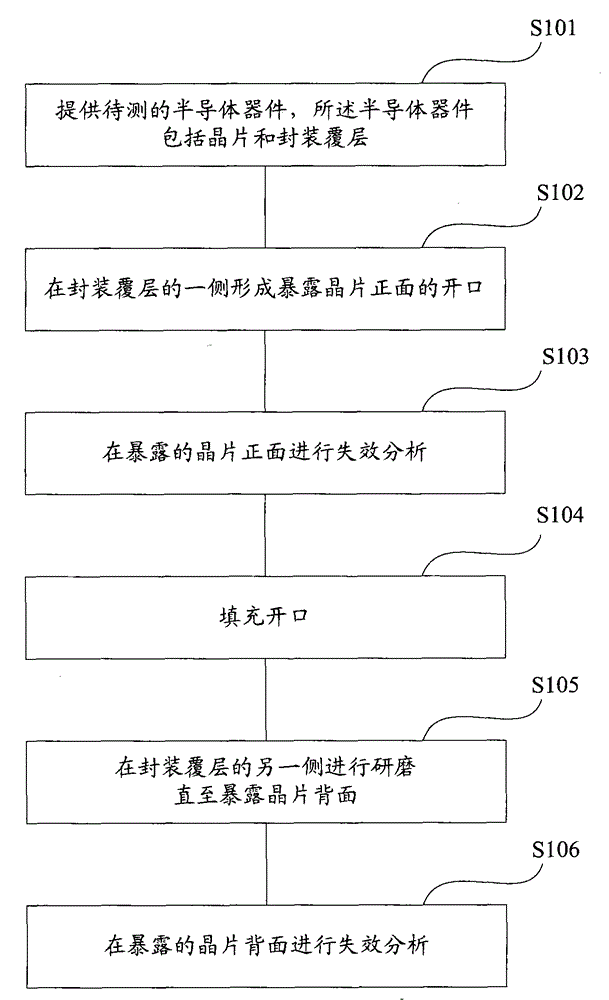
[0024] Therefore, in order to solve the above problems, such as figure 1 As shown, according to one embodiment of the present invention, a method for failure analysis in a semiconductor device is provided, comprising the steps of:

[0025] S101, providing a semiconductor device to be tested, the semiconductor device including a wafer and a packaging coating;

[0026] S102, forming an opening exposing the front surface of the chip on one side of the package coating;

[0027] S103, perf...


PUM


Abstract

The invention relates to a method for carrying out failure analysis in a semiconductor device, which comprises the following steps: providing the semiconductor device to be tested, wherein the semiconductor device comprises a wafer and an encapsulation cladding; forming an opening which makes the front side of the wafer exposed on one side of the encapsulation cladding; carrying out failure analysis on the exposed front side of the wafer; filling the opening; carrying out grinding on the other side of the encapsulation cladding to expose the back of the wafer; and carrying out failure analysis on the exposed wafer back. Compared with the prior art, the invention adopts the method of opening on the front side of the wafer firstly and then grinding on the back of the wafer, realizes once failure analysis respectively on the front side and the back of the wafer, improves the accuracy of the failure analysis, strengthens the effect of the failure analysis and improves the utilization rate of the wafer.

Description

technical field [0001] The invention relates to the technical field of semiconductors, in particular to a method for performing failure analysis in semiconductor devices. Background technique [0002] For the mass production of semiconductor devices, it is desirable to provide a profitable and reliable process technology. A process for improving reliability and stability of process technology includes the steps of designing a semiconductor device, manufacturing a sample of the semiconductor device, and testing the sample. Failure analysis of semiconductor devices is a feedback process that involves finding and correcting the root cause of defects to overcome the problems created by the defects. [0003] Proper failure analysis is critical to improving the quality of semiconductor devices. Incorrect failure analysis can lengthen the period required to develop and ramp up semiconductor device products. Generally, failure analysis includes external inspection, non-destructiv...

Claims


Application Information

Patent Timeline
Patent Type & Authority Patents(China)
IPC IPC(8): G01N21/88G01N13/10G01R31/303
Inventor 陈强郭志蓉周晶
Owner SEMICON MFG INT (SHANGHAI) CORP
Why Eureka
Try Eureka