Organic electroluminescence panel and manufacturing method thereof

A technology for electroluminescent panels and electroluminescent devices, which is applied in the manufacture of semiconductor/solid-state devices, circuits, electrical components, etc., can solve the problems of slow production speed, high process requirements, high production costs, etc. Overcome the effect of high requirements on alignment accuracy and simplify equipment and processes

Active Publication Date: 2013-01-23
BOE TECH GRP CO LTD
View PDF3 Cites 0 Cited by
  • Summary
  • Abstract
  • Description
  • Claims
  • Application Information

AI Technical Summary

Problems solved by technology

For position-overlapping laminated structure devices, the manufacturing scheme of the prior art needs to accurately align the positions of each layer in all directions of the substrate plane, and the error should be kept on the order of microns. This manufacturing method has high process requirements, resulting in high production costs. Larger, slow production speed, and low yield

Method used


Image

  • Organic electroluminescence panel and manufacturing method thereof
  • Organic electroluminescence panel and manufacturing method thereof
  • Organic electroluminescence panel and manufacturing method thereof

Examples


no. 1 example

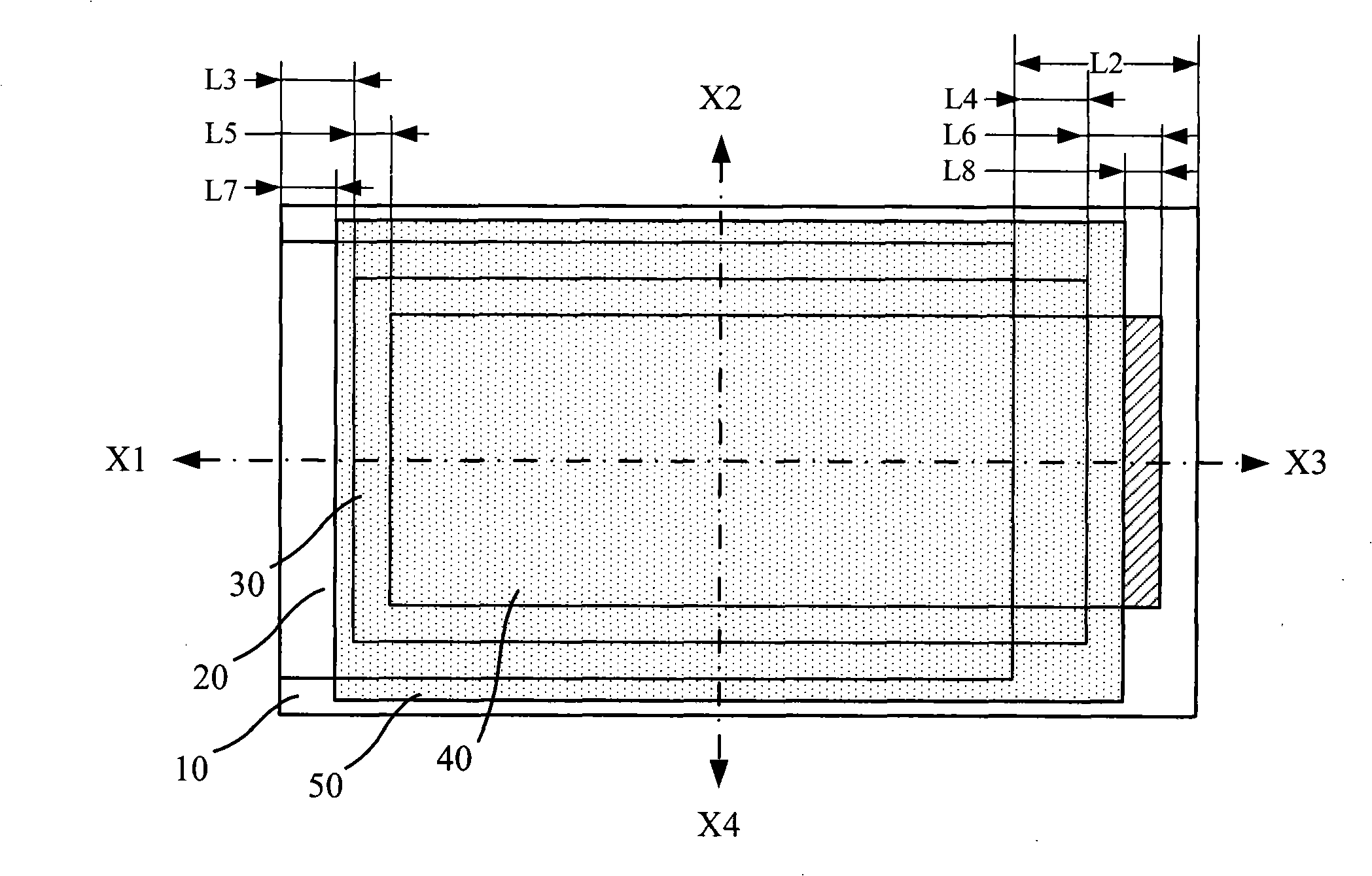
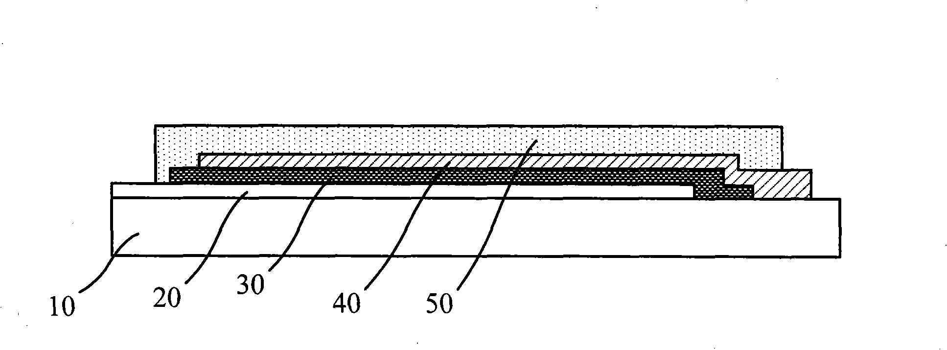
[0036] figure 1 It is a schematic top view structure diagram of the first embodiment of the organic electroluminescent panel of the present invention, figure 2 It is a side-view structure diagram of the first embodiment of the organic electroluminescence panel of the present invention. Such as figure 1 As shown, the organic electroluminescence panel mainly includes a substrate 10 , and a bottom electrode 20 , an organic layer 30 , a top electrode 40 and a sealing layer 50 are sequentially formed on the substrate 10 from bottom to top. For the sake of clarity of description, in the plane where the substrate 10 is located, it is considered that there are four directions respectively facing both ends of the horizontal axis and the vertical axis, that is, the first direction X1, the second direction X2, the third direction X3 and the fourth direction X4. In the example, the first direction X1 and the third direction X3 are respectively towards the two ends of the horizontal a...

no. 4 example

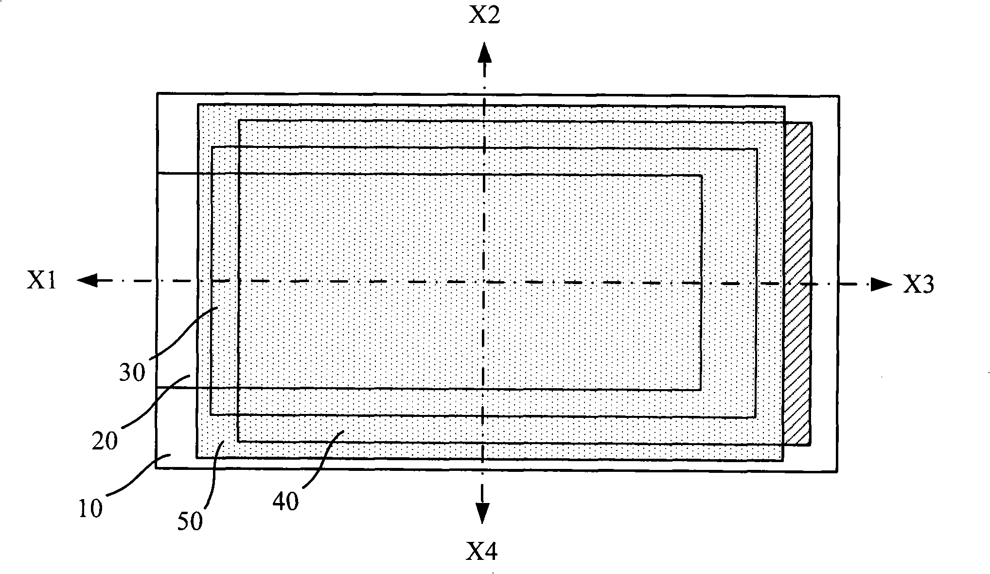
[0058] Figure 5 It is a top view structure schematic diagram of the fourth embodiment of the organic electroluminescence panel of the present invention. In this embodiment, the bottom electrode 20, the organic layer 30, the top electrode 40 and the sealing layer 50 stacked on the substrate 10 can be used as an organic electroluminescent device unit, and the substrate 10 corresponding to each organic electroluminescent device unit can be seen As a unit on the whole substrate 10, the setting of its edge is set according to the alignment requirements, then a plurality of organic electroluminescent device units can be formed in parallel on the whole substrate 10, such as Figure 5 shown.

[0059] It is also possible to form organic electroluminescent device units in series alone, or in combination of series and parallel. This embodiment is especially suitable for continuous production of organic electroluminescent panels in batches using a roll-to-roll manufacturing process, wh...


PUM


Abstract

The invention relates to an organic electroluminescence panel and a manufacturing method thereof. The organic electroluminescence panel comprises a base plate, a bottom electrode, an organic layer, a top electrode and a sealing layer, wherein the bottom electrode, the organic layer, the top electrode and the sealing layer are formed on the base plate from bottom to top; the distance between the edges of the bottom electrode, the organic layer and the top electrode in at least one direction and the edge of the base plate is increased progressively, and the distance between the edges of the bottom electrode, the organic layer and the top electrode in at least the other direction and the edge of the base plate is decreased progressively; the part of the top electrode overlapped above the bottom electrode is formed in the range of the organic layer; the sealing layer is covered on the bottom electrode, the organic layer and the top electrode, and at least part of the bottom electrode is exposed out in the distance-increased direction; and at least part of the top electrode is exposed out in the distance-decreased direction. The invention adopts a technical means that each layer structure on the organic electroluminescence panel relatively offsets for a certain distance, and can reduce the requirement of alignment accuracy. Accordingly, the invention can simplify equipment and process, can reduce cost, and can increase manufacturing speed and yield.

Description

technical field [0001] The invention relates to the manufacturing technology of an organic electroluminescent device, in particular to an organic electroluminescent plate and a manufacturing method thereof. Background technique [0002] An organic electroluminescent device is a device with a multilayer thin film structure, which can be used in the fields of display and lighting. Its basic structure includes a positive electrode and a negative electrode, and an organic layer sandwiched between the two electrodes. The light-emitting principle of organic electroluminescent devices is: when an appropriate voltage is applied between the positive electrode and the negative electrode, electrons and holes are respectively injected into the organic layer from the negative electrode and the positive electrode, and meet and recombine at a certain position in the organic layer. Release energy to glow. Wherein, the two electrodes and the organic layer can both be multi-layer structures,...

Claims


Application Information

Patent Timeline
Patent Type & Authority Patents(China)
IPC IPC(8): H01L51/50H01L51/56
Inventor 孙力
Owner BOE TECH GRP CO LTD
Why Eureka
Try Eureka