Light emitting diode and preparation method thereof

A technology for light-emitting diodes and light-emitting layers, which is applied in the manufacture of semiconductor/solid-state devices, electrical components, and electrical solid-state devices. Transport rate and hole transport rate, and the effect of improving efficiency

Active Publication Date: 2021-07-16
TCL CORPORATION
View PDF3 Cites 0 Cited by
  • Summary
  • Abstract
  • Description
  • Claims
  • Application Information

AI Technical Summary

Problems solved by technology

[0004] The main purpose of the present invention is to provide a light-emitting diode, aiming to solve the problem of unbalanced electron transfer rate and hole transfer rate in existing light-emitting diodes

Method used


Image

  • Light emitting diode and preparation method thereof
  • Light emitting diode and preparation method thereof
  • Light emitting diode and preparation method thereof

Examples


Embodiment approach

[0034] As an embodiment, the particle size of the noble metal nanoparticles is 30-50 nanometers.

[0035]In the embodiment of the present invention, the noble metal nanoparticles may be commercially available, or may be a product prepared by conventional techniques in the art.

[0036] In some embodiments, the noble metal nanoparticles are gold nanoparticles, and its preparation method includes:

[0037] (1) After washing, rinsing and drying with aqua regia, first add 100mL of pure water, then add 1mL of 0.5mmol / mL trisodium citrate solution;

[0038] (2) 20mL, 0.0025mmol / mL of HAuCl 4 and 10mL, 0.01mmol / ml CTAB (cetyltrimethylammonium bromide) mixed solution was quickly injected into the trisodium citrate solution, stirred vigorously for 1min, and stood at room temperature for 1h to obtain the precious metal seed solution;

[0039] (3) Add 5 mL, 0.01 mmol / ml CTAB, 5.5 mL, 0.01 mmol / ml chloroauric acid, 3 mL, 0.01 mmol / ml ascorbic acid into ultrapure water to obtain growth s...

Embodiment 1

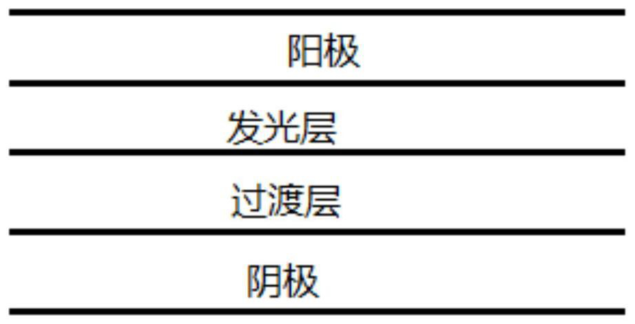
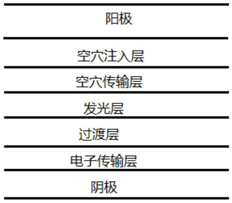
[0070] In this embodiment, a light-emitting diode is prepared, including an ITO bottom electrode, a hole injection layer, a hole transport layer, a quantum dot light-emitting layer, a transition layer, an electron transport layer, and a cathode that are sequentially stacked.

[0071] The method for preparing the above light-emitting diode specifically includes the following steps:

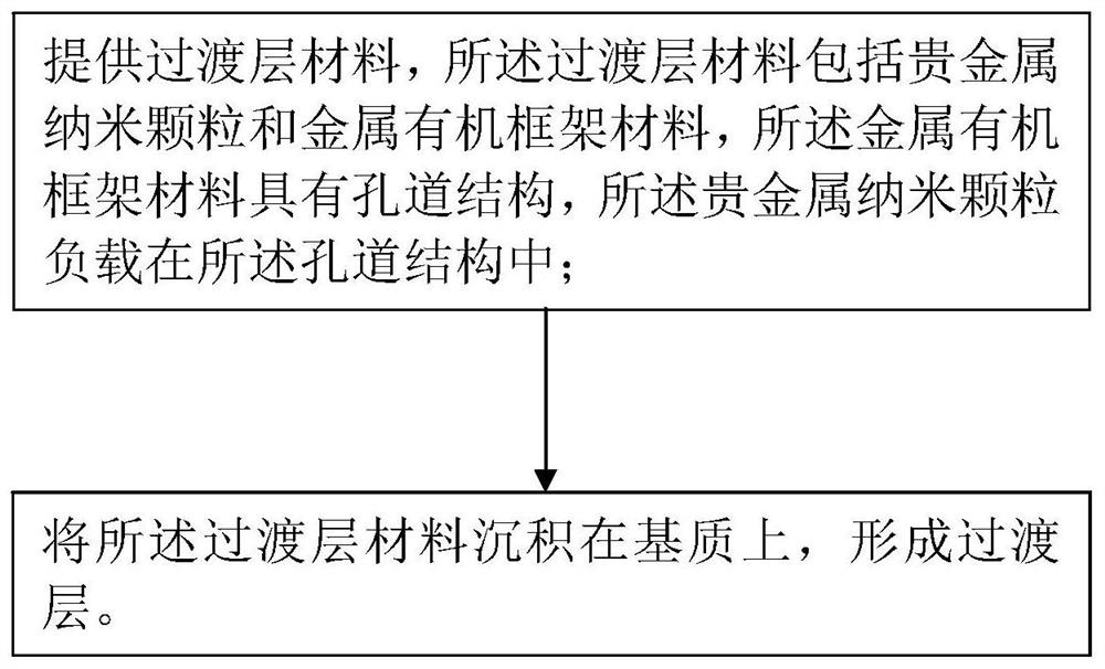
[0072] 1. Preparation of transition layer material

[0073](1) After washing, rinsing and drying with aqua regia, first add 100mL of pure water, then add 1mL of 0.5mmol / mL trisodium citrate solution;

[0074] (2) 20mL, 0.0025mmol / mL of HAuCl 4 and 10mL, 0.01mmol / ml CTAB (cetyltrimethylammonium bromide) mixed solution was quickly injected into the trisodium citrate solution, stirred vigorously for 1min, and stood at room temperature for 1h to obtain the precious metal seed solution;

[0075] (3) Add 5 mL, 0.01 mmol / ml CTAB, 5.5 mL, 0.01 mmol / ml chloroauric acid, 3 mL, 0.01 mmol / ml ascorbic acid in...

Embodiment 2

[0086] A light-emitting diode is prepared in this example, and the difference from Example 1 is that the thickness of the hole injection layer is 25 nanometers; the thickness of the cathode is 10 nanometers.


PUM

PropertyMeasurementUnit
particle diameteraaaaaaaaaa
thicknessaaaaaaaaaa
thicknessaaaaaaaaaa

Abstract

The invention belongs to the technical field of display, and particularly relates to a light-emitting diode and a preparation method thereof. The light-emitting diode provided by the invention comprises an anode, a cathode, a light-emitting layer arranged between the anode and the cathode, and a transition layer arranged between the cathode and the light-emitting layer, wherein the transition layer is made of noble metal nanoparticles and a metal organic framework material, the metal organic framework material has a pore channel structure, and the noble metal nanoparticles are loaded in the pore channel structure. According to the invention, the problem that the electron transmission rate and the hole transmission rate of an existing light-emitting diode are unbalanced is solved, and the light-emitting performance of the light-emitting diode is improved.

Description

technical field [0001] The invention belongs to the field of display technology, in particular to a light emitting diode and a preparation method thereof. Background technique [0002] Quantum Dot Light Emitting Diodes (QLED) is a new type of display device that uses quantum dots as light-emitting layer materials to apply to organic or polymer electroluminescent devices. Electrons and holes are injected into the light-emitting layer and passed through Radiation composite luminescence has the advantages of low cost, light weight, fast response speed, high color saturation, etc. It has broad development prospects and has become one of the important research directions of the new generation of LED display devices. [0003] However, in the current quantum dot light-emitting diodes, the electron transport rate is often greater than the hole transport rate, which leads to unstable electron and hole recombination in the light-emitting layer, and even causes excessive electron injec...

Claims


Application Information

Patent Timeline
Patent Type & Authority Applications(China)
IPC IPC(8): H01L51/50H01L51/56
CPCH10K50/00H10K50/115H10K50/16H10K71/00
Inventor 夏思雨杨一行
Owner TCL CORPORATION
Why Eureka
Try Eureka