[0020] The technical solutions of the present invention will be further described in detail below through the accompanying drawings and embodiments.
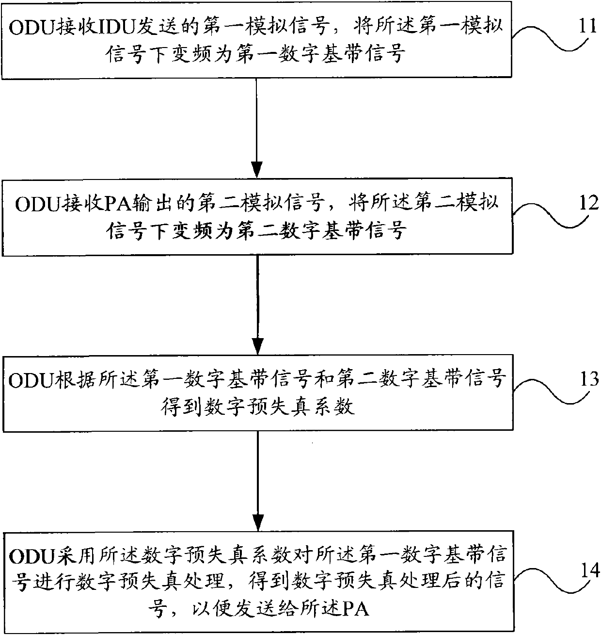
[0021] figure 1 A schematic flowchart of the method provided by the first embodiment of the present invention includes:
[0022] Step 11: The ODU receives the first analog signal sent by the IDU, and down-converts the first analog signal into a first digital baseband signal.
[0023] The IDU may send the first analog signal to the ODU through a multiplexer (Multiplexer) between the IDU and the ODU. The multiplexer can transmit signals in a variety of frequency bands and is isolated from each other. Usually, the IDU and the ODU are connected by a multiplexer. Of course, it can be understood that other devices with the same function as the multiplexer can also be used. .
[0024] Step 12: The ODU receives the second analog signal output by the PA, and down-converts the second analog signal into a second digital baseband signal.
[0025] Among them, a coupler can be used to divide the signal output from the PA into two channels, one channel is sent to the duplexer, and then sent to the microwave antenna through the duplexer to be sent to the other side; the other channel can be fed back from the PA output end .
[0026] Step 13: The ODU obtains a digital predistortion coefficient according to the first digital baseband signal and the second digital baseband signal.
[0027] The principle of digital predistortion (DPD) technology is generally as follows: before the signal enters the PA, the signal is firstly predistorted by using DPD coefficients. distorted purpose.
[0028] The DPD coefficient can be implemented by using various models, and specifically, the DPD coefficient can be obtained by using one of the existing technologies, which may not be limited here.
[0029] Step 14: The ODU performs digital pre-distortion processing on the first digital baseband signal by using the digital pre-distortion coefficient to obtain a digital pre-distortion processed signal for sending to the PA.
[0030] In this embodiment, by performing digital pre-distortion processing in the ODU, the linearization of the transmission chain can be realized without requiring that the PA must work in a linear mode. Therefore, the PA of this embodiment can work not only in the class A working mode belonging to the linear mode, but also in the class B working mode or the class AB working mode with poor linearity, so as to improve the working efficiency of the PA. Therefore, this embodiment can realize the linearization of the link, improve the working efficiency of the PA, and realize the improvement of the output performance.
[0031] figure 2 A schematic structural diagram of an ODU provided by the first embodiment of the present invention includes a first receiving module 21 , a second receiving module 22 , a computing module 23 and a digital predistortion module 24 . The first receiving module 21 is used for receiving the first analog signal sent by the IDU, and down-converting the first analog signal into a first digital baseband signal; the second receiving module 22 is used for receiving the second analog signal output by the power amplifier, converting the first analog signal into a first digital baseband signal. The second analog signal is down-converted into a second digital baseband signal; the calculation module 23 is connected with the first receiving module 21 and the second receiving module 22, and is used for obtaining according to the first digital baseband signal and the second digital baseband signal. digital pre-distortion coefficient; the digital pre-distortion module 24 is configured to perform digital pre-distortion processing on the first digital baseband signal by using the digital pre-distortion coefficient to obtain a digital pre-distortion processed signal for sending to the power amplifier.
[0032] In this embodiment, by performing digital pre-distortion processing in the ODU, the linearization of the transmission link can be realized without requiring the PA to work in the linear mode. The PA in this embodiment can work in the class A working mode and the class B working mode. Or in the class AB working mode, improve the working efficiency of the PA. Since the linearization of the link can be realized and the linearity of the PA is not required, it can not only ensure that the signal is not distorted, but also ensure that the specific working efficiency of the PA is better, so as to realize the improvement of the output performance.
[0033] In order to better adapt to changes in the environment, the working mode of the PA in this embodiment may also adopt an adaptive adjustment manner.
[0034] image 3 It is a schematic flowchart of the method provided by the second embodiment of the present invention, Figure 4 This is a schematic structural diagram of an ODU provided by the second embodiment of the present invention.
[0035] see Figure 4 , the ODU provided in this embodiment includes a first receiving module 41 , a second receiving module 42 , a computing module 43 and a digital predistortion module 44 , and the specific functions of the above modules may refer to the first embodiment.
[0036] This embodiment also includes a processing module 45 and a PA 46. The processing module 45 is used to perform digital-to-analog conversion and modulation frequency shifting on the digitally predistorted signal to obtain a third analog signal; the PA 46 is used to receive the digital-to-analog signal. The third analog signal is obtained, and the second analog signal is obtained after power amplification is performed on the third analog signal.
[0037] The carrier frequency of the first analog signal may be an intermediate frequency frequency F0, and the first receiving module 41 may include a first digital down converter (Digital Down Converter, DDC) 411, and the first DDC 411 is used to receive the first analog signal sent by the IDU , and the intermediate frequency F0 is used as the local oscillator frequency Lo1, and the intermediate frequency is used to down-convert the first analog signal into a first in-phase digital signal I1 and a first quadrature digital signal Q1.
[0038] The signals after the digital pre-distortion process are the in-phase digital signal I1' after the digital pre-distortion process and the quadrature digital signal Q2' after the digital pre-distortion process; the processing module 45 includes a first digital-to-analog converter (Digital Analog Converter). Converter, DAC) 451 , a first Low Pass Filter (LPF) 452 , a second DAC 453 , a second LPF 454 , an IQ modulator 455 and a first mixer 456 . The first DAC 451 is configured to perform digital-to-analog conversion on the in-phase digital signal after the digital predistortion process to obtain a first transmitted analog signal; the first LPF 452 is configured to perform low-pass filtering on the first transmitted analog signal to obtain The first low-pass filter processed signal; the second DAC 453 is used to perform digital-to-analog conversion on the quadrature digital signal after the digital pre-distortion process to obtain a second transmitted analog signal; the second LPF 454 is used to The second sending analog signal is low-pass filtered to obtain a second low-pass filtered signal; the IQ modulator 455 is used to directly modulate the signal to the intermediate frequency F0, and use the intermediate frequency to process the first low-pass filtering The latter signal and the second low-pass filtered signal are modulated into a fourth analog signal whose frequency is the intermediate frequency; the first mixer (Mixer) 456 converts the intermediate frequency to the microwave frequency Lo2, and Lo2 is used as the microwave frequency. The local oscillator frequency is used to up-convert the fourth analog signal into the third analog signal by using the radio frequency, and the carrier frequency of the third analog signal is the microwave frequency Lo2.
[0039]The second receiving module 42 may include a second mixer 421, a Band Pass Filter (BPF) 422 and a second DDC 423. The second mixer 421 is configured to receive the second analog signal output by the power amplifier, Specifically, the coupler 47 can be used to divide the signal output from the PA into two channels, and one channel is sent to the second mixer 421. The second mixer 421 converts the RF frequency to an intermediate frequency, where Lo2 is used as the local oscillator frequency, using The radio frequency down-converts the second analog signal into a fifth analog signal, and the carrier frequency of the fifth analog signal is the intermediate frequency F0 (the same frequency F0 as the transmitting frequency can be selected here, and the local oscillator can be shared. frequency source); the band-pass filter 422 is used to perform band-pass processing on the fifth analog signal to obtain the analog signal after the band-pass filter processing; the second DDC 423 is used to directly digitally down-convert the intermediate frequency F0, A second in-phase digital signal I2 and a second quadrature digital signal Q2 are obtained.
[0040] This embodiment may further include a correction module 48, and the correction module 48 is configured to perform analog quadrature modulation (Analog Quadrature Modulation, AQM) and correction processing on the digitally predistorted signal. Wherein, the calculation module 43 , the digital predistortion module 44 and the correction module 48 may be integrated on a field programmable gate array (Field Programmable Gate Array, FPGA) 49 .
[0041] For the connection relationship between the above modules, please refer to Figure 4 shown. The above-mentioned F0 and Lo1 can be specifically 350M.
[0042] see image 3 , the method provided by this embodiment includes:
[0043] Step 301: The first DDC in the ODU receives the first analog signal sent by the IDU, and the carrier frequency of the first analog signal is the intermediate frequency frequency F0.
[0044] Step 302: The first DDC in the ODU uses the intermediate frequency F0 as the local oscillator frequency, and down-converts the first analog signal into a first in-phase digital signal I1 and a first quadrature digital signal Q1.
[0045] Step 303: The digital predistortion module in the ODU performs digital predistortion processing on the first in-phase digital signal I1 and the first quadrature digital signal Q1 to obtain the digital predistortion processed in-phase digital signal I1' and digital predistortion The processed quadrature digital signal Q 1'.
[0046] Step 304: The first DAC in the ODU performs digital-to-analog conversion on I1' to obtain one channel of digital-to-analog converted signals.
[0047] Step 305: The first LPF in the ODU performs low-pass filtering on the digital-to-analog converted signal to obtain a low-pass filtered signal.
[0048] Step 306: The second DAC in the ODU performs digital-to-analog conversion on Q1' to obtain another signal after digital-to-analog conversion.
[0049] Step 307: The second LPF in the ODU performs low-pass filtering on the other channel of digital-to-analog converted signals to obtain another channel of low-pass filtered signals.
[0050] Steps 304-305 and steps 306-307 have no timing restriction relationship.
[0051] Step 308: The modulator in the ODU uses the intermediate frequency F0 as the local oscillator frequency of the modulator, and modulates the two analog signals into a fourth analog signal whose carrier frequency is the intermediate frequency.
[0052] Step 309: The first mixer in the ODU uses the microwave frequency Lo2 as the local oscillator frequency, and up-converts the fourth analog signal into a third analog signal, and the carrier frequency of the third analog signal is the microwave frequency Lo2 .
[0053] Step 310: The first mixer sends the third analog signal to the PA in the ODU.
[0054] Step 311: After the PA performs power amplification processing on the third analog signal, a second analog signal is obtained.
[0055] Step 312: The coupler in the ODU divides the second analog signal into two channels, one channel is sent to the duplexer, and then sent to the microwave antenna through the duplexer; the other channel is fed back to the second mixer in the ODU.
[0056] Step 313: The second mixer uses the microwave frequency Lo2 as the local oscillator frequency, and down-converts the second analog signal into a fifth analog signal, the carrier frequency of which is equal to the intermediate frequency F0.
[0057] Step 314: The BPF in the ODU performs bandpass processing on the fifth analog signal to obtain a bandpass filtered analog signal.
[0058] Step 315: The second DDC uses the intermediate frequency F0 as the local oscillator frequency, and down-converts the band-pass filtered analog signal into a second in-phase digital signal I2 and a second quadrature digital signal Q2.
[0059] Step 316: The calculation module in the ODU obtains a digital predistortion coefficient according to the first digital baseband signal (I1, Q1) and the second digital baseband signal (I2, Q2).
[0060] Step 317: The digital predistortion module in the ODU uses the digital predistortion coefficient to perform digital predistortion processing on the first digital baseband signal to obtain a digital predistortion processed signal.
[0061] Step 318: The correction module in the ODU performs amplitude quadrature modulation (AQM) and correction processing on the digital predistorted signal to obtain updated I1' and Q1'.
[0062] Of course, it can be understood that the correction processing can also be performed first, and then the digital predistortion processing can be performed.
[0063] After that, steps 304-318 can be repeatedly performed to form a continuous closed-loop DPD, and then adaptive processing can be implemented to adapt to changes in the environment.
[0064] In this embodiment, by performing digital pre-distortion processing in the ODU, the linearization of the transmission link can be realized without requiring the PA to work in the linear mode. The PA in this embodiment can work in the class B working mode or the class AB working mode. (or you can bias the class A power amplifier to class AB) to improve the working efficiency of the PA and save energy. Moreover, in this embodiment, a closed-loop DPD can be formed through the above-mentioned cycle. Compared with an open-loop DPD or a static DPD, the closed-loop DPD has a larger and more stable income, and can be adaptively adjusted according to different output powers. Therefore, it can reduce the The requirements for production debugging, improve the pass-through rate and reduce the impact of the environment on the PA. Therefore, the present embodiment can ensure the performance of the system and improve the competitiveness of the product.
[0065] Those of ordinary skill in the art can understand that all or part of the steps of implementing the above method embodiments may be completed by program instructions related to hardware.
[0066] The descriptions such as "first" and "second" in the embodiments of the present invention are only for making the description clearer, and do not indicate the pros and cons of the solution.
[0067] Finally, it should be noted that the above embodiments are only used to illustrate the technical solutions of the present invention rather than limit them. Although the present invention has been described in detail with reference to the preferred embodiments, those of ordinary skill in the art should understand that: it is still The technical solutions of the present invention may be modified or equivalently replaced, and these modifications or equivalent replacements cannot make the modified technical solutions depart from the spirit and scope of the technical solutions of the present invention.