

Pixel structure
A technology of pixel structure and pixel capacitance, applied in the field of pixel structure, can solve the problem that the pixel unit cannot work normally
- Summary
- Abstract
- Description
- Claims
- Application Information
AI Technical Summary
Problems solved by technology
Method used
Image

Examples
Embodiment Construction
[0026] In the drawings, when an element is referred to as being “connected” or “coupled” to another element, it may be directly connected or coupled to the other element or intervening elements may be present. In contrast, when an element is referred to as being "directly connected" or "directly coupled" to another element, there are no intervening elements present.
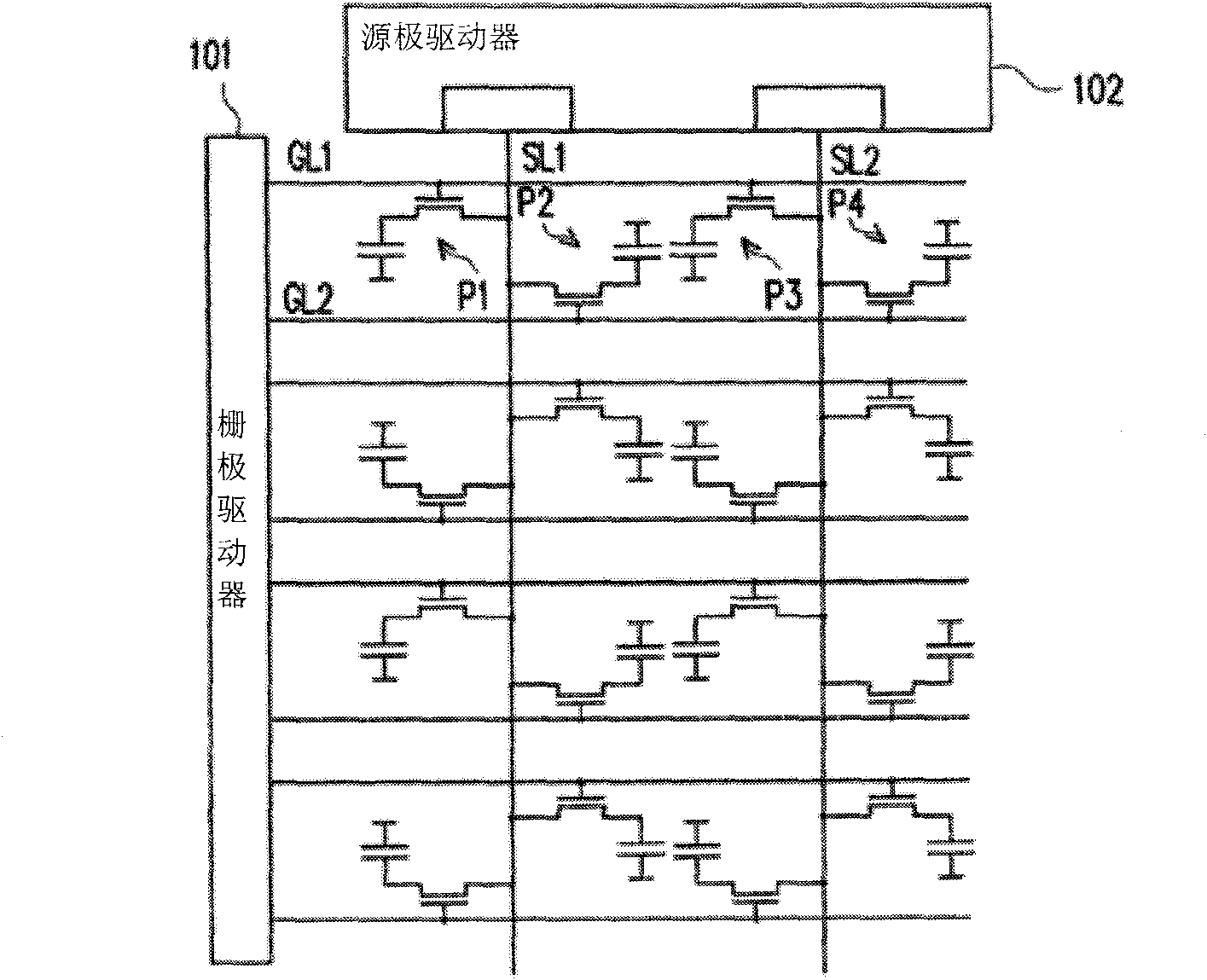
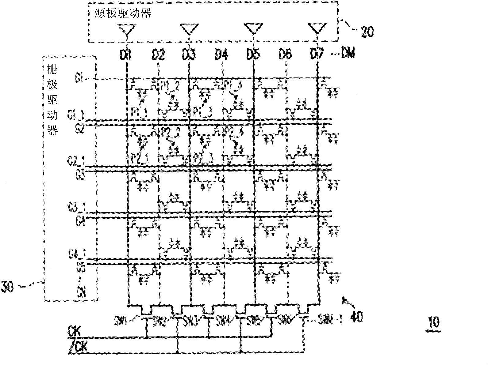
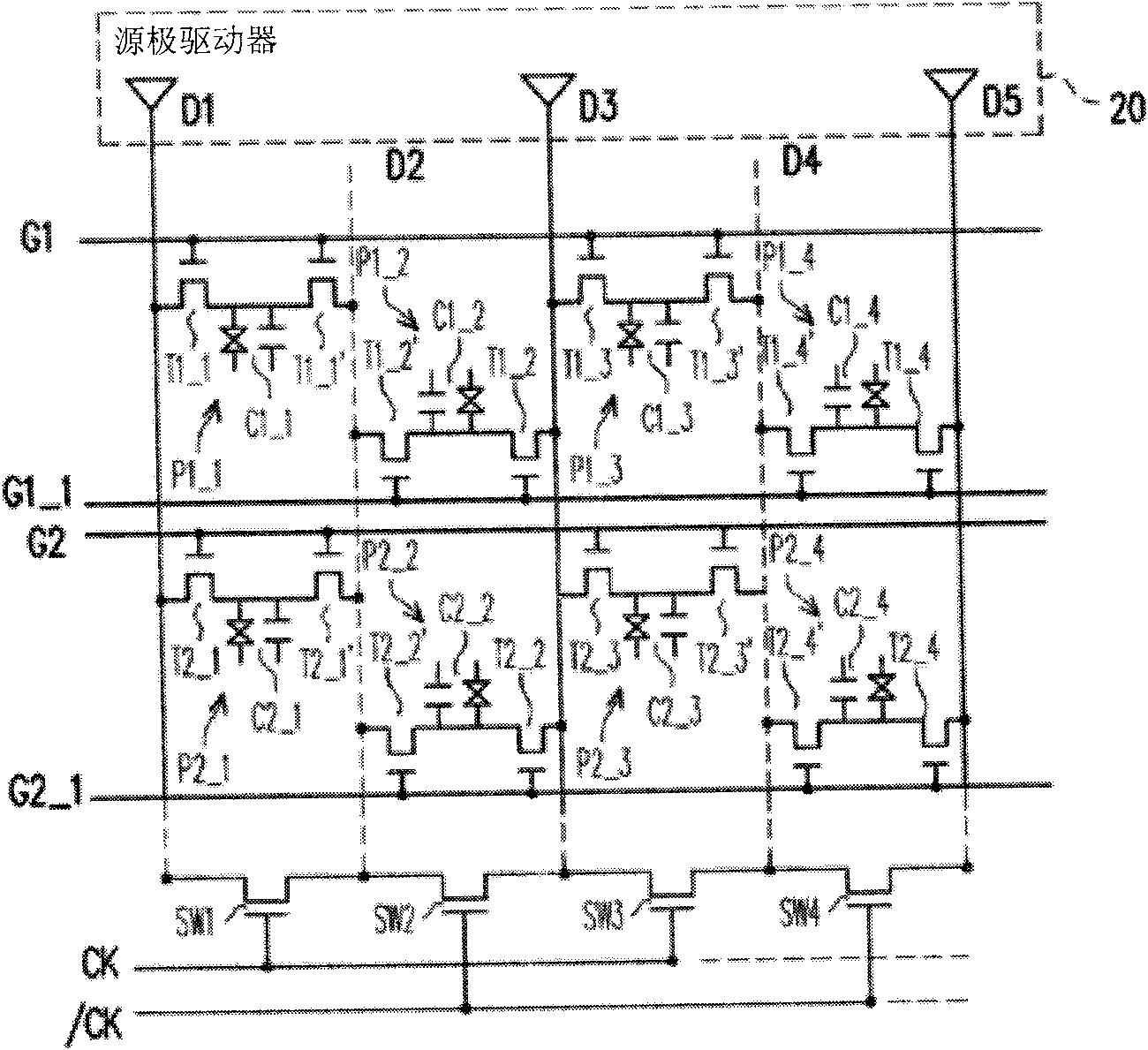
[0027] figure 2 is a schematic diagram of a liquid crystal display according to the first embodiment of the present invention. Figure 3A yes figure 2 A partial enlargement of the . Figure 3B yes figure 2 A partial layout diagram of . Please merge reference figure 2 , Figure 3A ,and Figure 3B . The liquid crystal display 10 includes a source driver 20, a gate driver 30, source lines D1-DM, gate lines G1, G1_1, G2, G2_1-GN, control switches SW1-SWM-1 and a pixel array 40, wherein N, M are natural numbers, and G1, G2, G3, . . . are odd-numbered gate lines, and G1_1, G2_1, G3_1, . . . are even-number...
PUM
 Abstract
Description
Claims
Application Information