Crystal grain angle correction method applied to chip separating system
A sorting system and angle correction technology, applied in sorting and other directions, can solve the problems of affecting the speed of die angle correction, reducing the speed of chip sorting, and difficulty in precise positioning of die.
- Summary
- Abstract
- Description
- Claims
- Application Information
AI Technical Summary
Problems solved by technology
Method used
Image
Examples
Embodiment 1
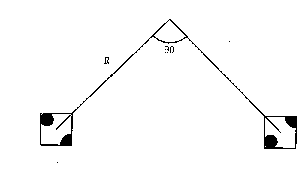
[0082] An embodiment of a grain angle correction method applied to a chip sorting system of the present invention is as follows figure 1 Shown is a flow chart of a method of the present invention.
[0083] Specifically, a grain angle correction method applied to a chip sorting system, wherein the chip sorting system includes an image recognition system, a chip feeding table, a grain transfer mechanism and an arrangement area, and the image recognition system includes A high-speed camera, the chip feeding platform includes an XY cross platform, a thimble and a Z-axis rotating platform, wherein the method includes the following steps:
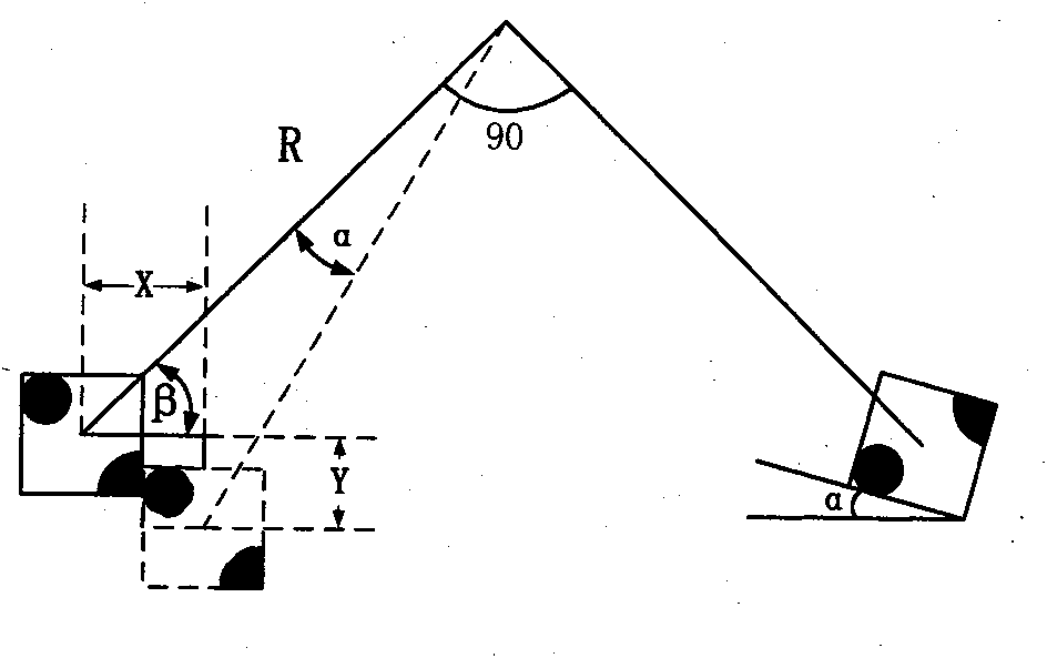
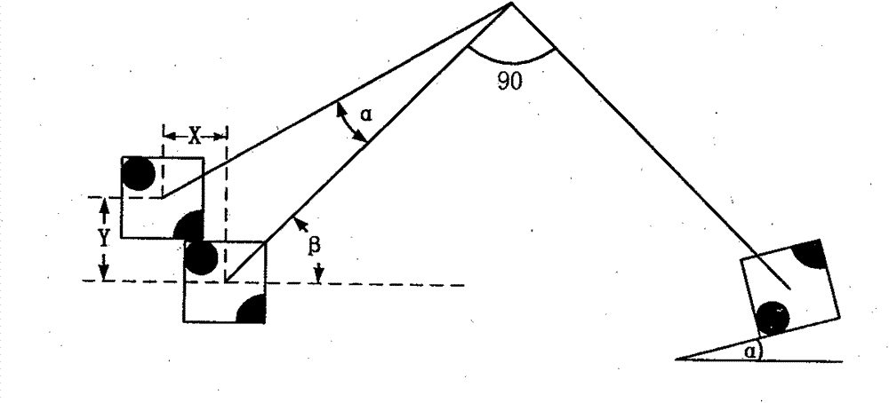
[0084] Step 101, setting the deflection range parameter of the allowable grain angle in the chip sorting system; wherein, this parameter can select different deflection range values according to the needs of the user, and the deflection range of the allowable grain angle commonly used in the industry It is -15°~+15° or -9°~+9°.
[0085] Step ...
Embodiment 2
[0111] An embodiment of a grain angle correction method applied to a chip sorting system of the present invention is as follows figure 2 Shown is another method flow chart of the present invention.
[0112] Specifically, a grain angle correction method applied to a chip sorting system, wherein the chip sorting system includes an image recognition system, a chip feeding table, a grain transfer mechanism and an arrangement area, and the image recognition system includes A high-speed camera, the chip feeding platform includes an XY cross platform, a thimble and a Z-axis rotating platform, wherein the method includes the following steps:
[0113] Step 201, setting the allowable deflection range parameters of the grain angle in the chip sorting system.
[0114] Step 202, selecting one of the dies on the chip film as the target die.
[0115] Step 203, drive the XY cross platform of the chip feed table to move the target die to the recognition area of the lens of the high-speed ...
PUM
 Abstract
Description
Claims
Application Information
 - R&D
- Intellectual Property
- Life Sciences
- Materials
- Tech Scout
- Unparalleled Data Quality
- Higher Quality Content
- 60% Fewer Hallucinations
Browse by: Latest US Patents, China's latest patents, Technical Efficacy Thesaurus, Application Domain, Technology Topic, Popular Technical Reports.
© 2025 PatSnap. All rights reserved.Legal|Privacy policy|Modern Slavery Act Transparency Statement|Sitemap|About US| Contact US: help@patsnap.com


