Optimization method of optical proximity correction rule

A technology for optical proximity correction and optimization methods, which is applied in optics, originals for opto-mechanical processing, and photoengraving processes of patterned surfaces. effect of time and manpower

Active Publication Date: 2010-07-28
SEMICON MFG INT (SHANGHAI) CORP
View PDF0 Cites 15 Cited by
  • Summary
  • Abstract
  • Description
  • Claims
  • Application Information

AI Technical Summary

Problems solved by technology

[0005] The technical problem to be solved by the present invention is that the correction rules used in the existing optical neighbor correction process are too simple, so that further adjustment and correction are still required in the actual correction process, which wastes a lot of time, manpower and energy

Method used


Image

  • Optimization method of optical proximity correction rule
  • Optimization method of optical proximity correction rule
  • Optimization method of optical proximity correction rule

Examples


Embodiment Construction

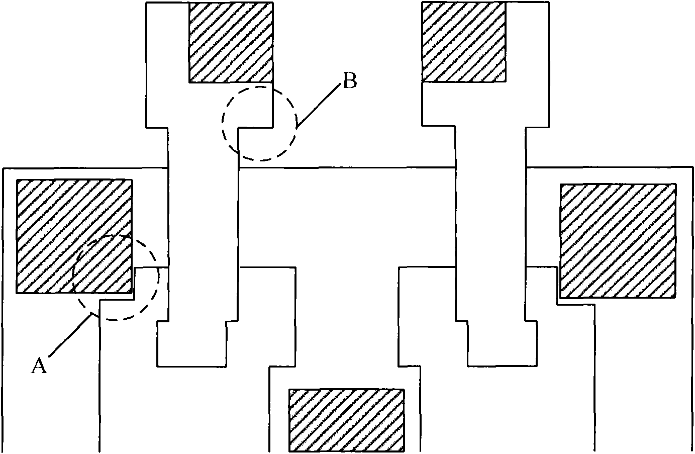
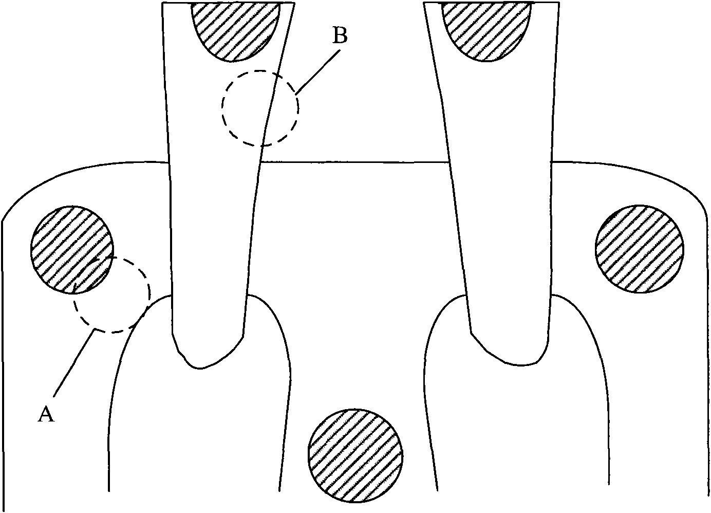
[0030] Due to the continuous shrinking of the device size, the influence of light on the actual layout pattern cannot be ignored more and more. refer to figure 1 and figure 2 , figure 1 is a design diagram of a byte unit of a static random access memory, figure 2 It is the simulation result obtained after performing optical model simulation on it. Compared figure 1 and figure 2 , in area A, it can be found that due to the optical and chemical effects in the actual manufacturing process, the inner corner will be passivated and rounded, and the increased area of ​​the inner corner will make the passivation of the inner corner more serious, which will affect the channel length of the adjacent transistor ; while in the B region, the small corners on the gate layer pattern are too small to be away from the space of the diffusion region, and the square corner passivation caused by the corners will also affect the width of the transistor.

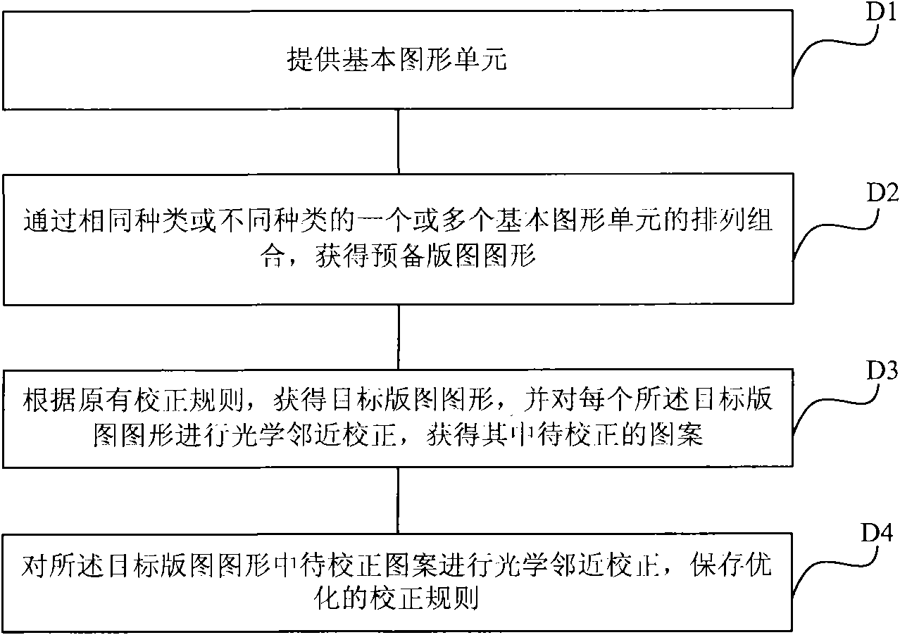
[0031] The present invention obtai...


PUM


Abstract

The invention discloses an optimization method of an optical proximity correction rule, comprising the following steps of: providing a basic graphics unit; arranging and combining one or a plurality of basic graphics units of the same kind or different kinds, and acquiring a preliminary domain graphics; acquiring the target domain graphics according to the traditional correction rule, carrying out the optical proximity correction on each target domain graphics and acquiring a pattern to be corrected; and correcting the pattern to be corrected in the target domain graphics and storing the optimized correction rule. The invention provides a large number of patterns with variety and randomness by the preliminary domain graphics consisting of the basic graphics unit and acquires the set of the correction rule corresponding to various patterns based on the optical proximity correction of the preliminary domain graphics; therefore, the optimization of the traditional correction rule is realized, and the time and the labor in the actual correction course are greatly saved.

Description

technical field [0001] The invention relates to optical proximity correction technology, in particular to an optimization method for optical proximity correction rules. Background technique [0002] With the rapid development of integrated circuit design, how to reduce the deformation and deviation of layout patterns after lithography, suppress the negative effects of optical proximity effect, and improve the yield of chip production plays a key role in the development of chip manufacturing industry. Aiming at this problem, a method commonly used in the industry at present is optical proximity correction, which reduces the deviation of the lithography pattern obtained by exposure by changing the shape of the original layout pattern. [0003] In the prior art, the process of optical proximity correction generally includes: optically simulating the original layout graphic to obtain a simulated graphic that simulates its image; by comparing the obtained simulated graphic with t...

Claims


Application Information

Patent Timeline
Patent Type & Authority Applications(China)
IPC IPC(8): G03F1/14G03F1/36
Inventor 张飞
Owner SEMICON MFG INT (SHANGHAI) CORP
Why Eureka
Try Eureka