Gain filter circuit applicable to scientific-grade CCDs

A filter circuit, scientific-level technology, applied in gain control, television, electrical components, etc., to achieve the effect of solving complex control and continuously adjustable gain

Inactive Publication Date: 2010-08-11
CENT FOR SPACE SCI & APPLIED RES
View PDF0 Cites 6 Cited by
  • Summary
  • Abstract
  • Description
  • Claims
  • Application Information

AI Technical Summary

Problems solved by technology

With the increasing application of astronomical observation cameras in space, due to the limitation of satellite resources, it is hoped that the camera can achieve gain adjustment in a simple and reliable way, and the shortcomings of the above circuit structure are becoming more and more obvious

Method used


Image

  • Gain filter circuit applicable to scientific-grade CCDs
  • Gain filter circuit applicable to scientific-grade CCDs
  • Gain filter circuit applicable to scientific-grade CCDs

Examples


Embodiment Construction

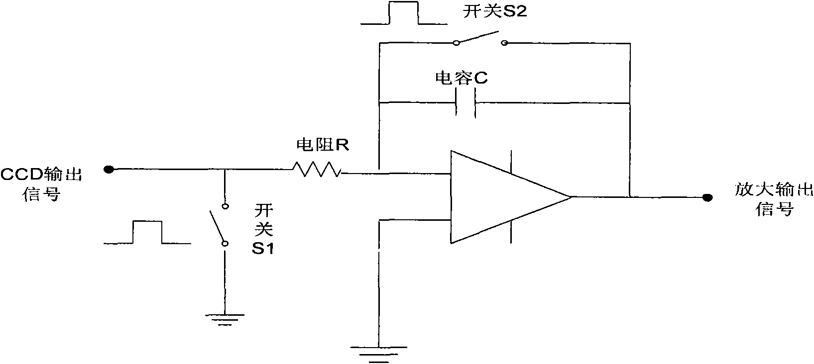
[0012] The gain filter circuit applied to a scientific grade CCD of the present invention will be described in detail below in conjunction with the accompanying drawings and specific embodiments.

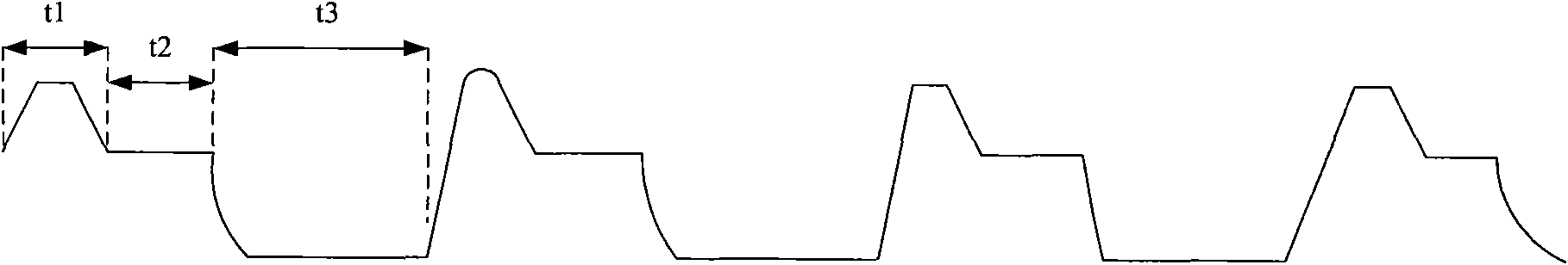
[0013] Applying the present invention to an astronomical observation camera using a scientific-grade CCD is based on the imaging principle of a scientific-grade CCD: the CCD is composed of pixels arranged in rows and columns, the image signals are stored in the pixels, and the output of the signal is driven sequentially by the drive signal in rows and columns. The CCD output terminal outputs in turn by pixel. At present, scientific-grade CCDs all adopt the output structure of floating diffusion amplifier, and the output structure of CCD determines the form of the signal. figure 1 is a scientific grade CCD output signal legend, such as figure 1 As shown, the output signal of each pixel of the CCD can be divided into three parts t1, t2, and t3 in time order. Among them, the t1 part i...


PUM


Abstract

The invention provides a gain filter circuit applicable to scientific-grade CCDs (charge coupled device), in particular to the processing circuit of CCDs. The gain filter circuit comprises an operational amplifier, two analog switches (S1 and S2), a resistor (R) and a capacitor (C), wherein the analog switch S2 is connected with the capacitor (C) in parallel to jointly form the negative feedback of the operational amplifier; the non-inverting input terminal of the operational amplifier is grounded, and the inverting input terminal thereof is connected with the output signal of the CCD via the resistor (R); and the output signal of the CCD is grounded via the other analog switch (S1). Followed by the start of the driving circuit of the CCD, the gain filter circuit can continuously adjust the amplification of the circuit on a real-time basis by adjusting and feeding back the disconnection time of the analog switch (S2) according to the driving timing sequence of the CCD; and by adjusting the capacitance of the capacitor (C) and the resistance of the resistor (R), the gain filter circuit can vary the amplification within a large range and vary the cutoff frequency of the circuit, thus achieving the low-pass filter on the output signals of the CCD. Accordingly, based on the simple control, the invention can achieve the continuously adjustable gain and the filter function.

Description

technical field [0001] The invention relates to the design of a control circuit of a camera, in particular to a design of a gain filter circuit applied to a scientific grade CCD. Background technique [0002] When performing astronomical observations, sometimes it is necessary to adjust the gain of the camera according to the radiation intensity of different observation targets, so that the dynamic range of the camera can be fully utilized for targets with different radiation intensities to obtain clear images, or for the same observation target, by adjusting the camera Gain, to observe the details of areas with different radiation intensities, and enhance the contrast of local images. At the same time, astronomical observation cameras all need filter circuits to obtain low-noise images. The currently used controllable gain circuit is implemented in two ways, one is to directly apply a programmable gain amplifier, and the other is to use a combination of an analog switch an...

Claims


Application Information

Patent Timeline
Patent Type & Authority Applications(China)
IPC IPC(8): H04N5/30H03G3/20
Inventor 彭吉龙朱光武李保权张鑫韦飞
Owner CENT FOR SPACE SCI & APPLIED RES
Why Eureka
Try Eureka