A time-sharing digital error correction circuit for a high-speed pipelined analog-to-digital converter
An analog-to-digital converter and error correction circuit technology, applied in the direction of analog-to-digital converter, analog/digital conversion calibration/test, etc. The effect of small amount, reduced circuit design complexity, and short delay
- Summary
- Abstract
- Description
- Claims
- Application Information
AI Technical Summary
Problems solved by technology
Method used
Image
Examples
specific Embodiment 1
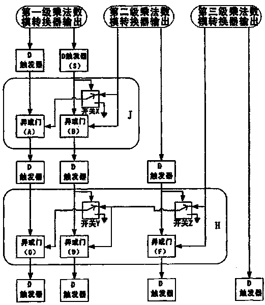
[0019] Specific embodiment one: the time-sharing digital error correction circuit of the analog-to-digital converter of four-bit precision sees image 3 , which includes a three-stage multiplication digital-to-analog converter, the high and low bits of the output of the first-stage multiplication digital-to-analog converter are respectively connected to their corresponding D flip-flops, and the D flip-flops connected to the first-stage high bits are connected to the exclusive OR gate (A) input end, the D flip-flop (S) connected to the first-level low-level connection is connected to the input terminal of the exclusive OR gate (B), the high-level output of the second-level multiplication digital-to-analog converter is connected to the input terminal of the exclusive-or gate (B), and the first-level low-level connection After the D flip-flop (S) and the high output of the second-stage multiplication digital-to-analog converter are respectively connected to the input terminal of t...
specific Embodiment 2
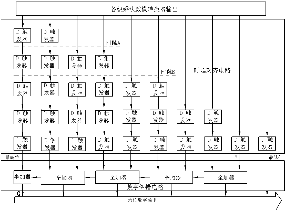
[0022] Specific embodiment two: the last stage of the time-sharing digital error correction circuit of the analog-to-digital converter of six-bit precision sees Figure 4 , which includes the D flip-flop corresponding to the output of the first five bits obtained by the above four-level operation, except that the highest D flip-flop is only connected to the input terminal of the XOR gate, and the flip-flops corresponding to the other four bits are connected to other The input end of the corresponding XOR gate and the input end of the corresponding switch, the output high bit of the final multiplication digital-to-analog converter is connected to the input end of the XOR gate connected to the fifth flip-flop and the input end of the switch, and then The output terminals of the first-level switch are respectively connected to the input terminals of the previous-level switch, the input terminal of the previous-level XOR gate until the next highest level, and the switch output corr...
PUM
 Abstract
Description
Claims
Application Information


