

Inorganic-organic semiconductor combined element having transverse photovoltaic effect and preparation method thereof
A technology of organic semiconductors and inorganic semiconductors, applied in semiconductor/solid-state device manufacturing, semiconductor devices, electric solid-state devices, etc., can solve the problems of low cost, large adjustable area, etc., and achieve materials simplification, variety, and cost reduction Effect
Inactive Publication Date: 2010-08-25
FUDAN UNIV
View PDF1 Cites 12 Cited by
- Summary
- Abstract
- Description
- Claims
- Application Information
AI Technical Summary
Problems solved by technology
The object of the present invention is to provide an inorganic-organic semiconductor composite device with a large adjustable area and relatively low cost and a lateral photovoltaic effect and its preparation method
Method used
View moreImage
Smart ImageViewing Examples


Examples
Embodiment 1
Embodiment 2
Embodiment 3
Login to View More PUM
| Property | Measurement | Unit |
|---|---|---|
| Thickness | aaaaa | aaaaa |
| Sensitivity | aaaaa | aaaaa |
Abstract
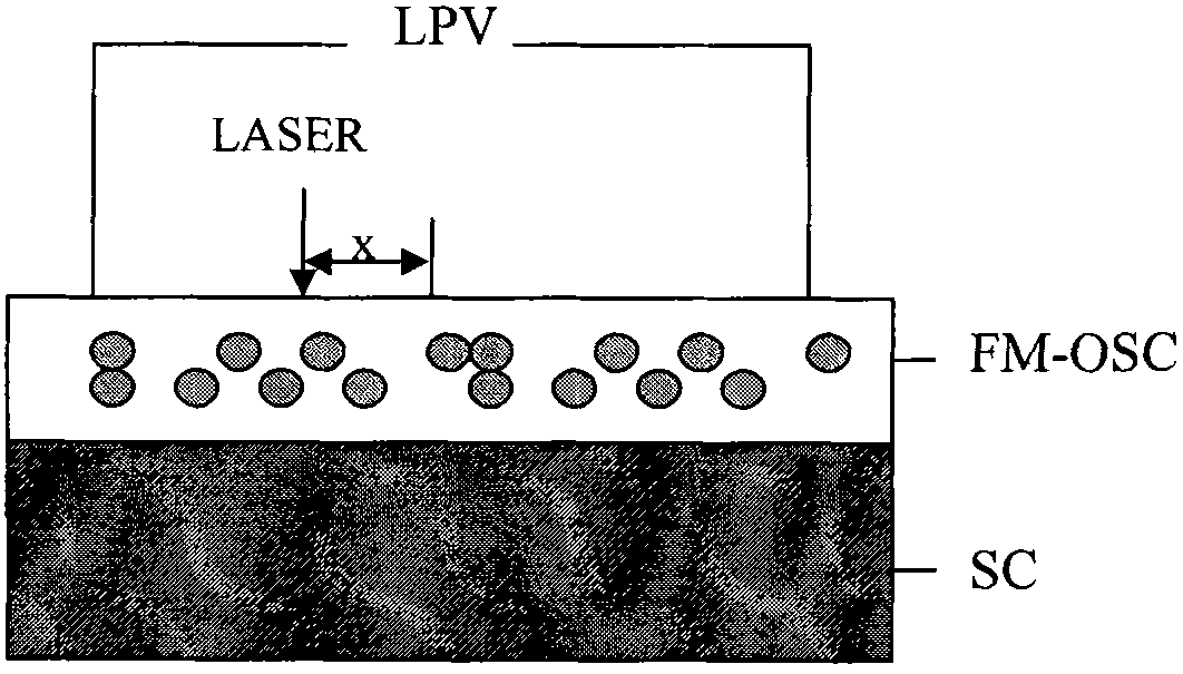
The invention belongs to the technical field of material preparation and sensors, in particular to an inorganic-organic semiconductor combined element having a transverse photovoltaic effect and a preparation method thereof. The element is prepared by depositing a magnetic metal material and an organic semiconductor material on an inorganic semiconductor substrate by means of coevaporation. The nano particles of the magnetic metal material are embedded in an organic semiconductor base and a composite nanoparticle membrane layer formed is expressed by a formula: (A)*(B)1-x, wherein x ranges from 0.3 to 0.9; A represents the magnetic metal material and B represents the organic semiconductor material; and the element structure is expressed as (A)*(B)1-x / Si or (A)*(B)1-x / SiO2 / Si. The element can be widely used elements such as position sensors.
Description
An inorganic organic semiconductor composite device with lateral photovoltaic effect and its preparation method technical field The invention belongs to the field of material preparation and sensor technology, and specifically relates to a newly discovered inorganic-organic semiconductor composite device with a lateral photovoltaic effect and a preparation method thereof, as well as applications in the fields of position sensors and the like. Background technique The lateral photovoltaic effect refers to the photovoltaic effect along the surface generated by the p-n junction, semiconductor heterojunction or metal semiconductor junction under point lighting, which can be applied to position sensitive detectors, rotary shaft encoders, x-y axis positioners and Optical positioning sensors, etc. At present, the most widely used ones are still based on traditional p-n junctions or metal-semiconductor junctions (MS) or metal-oxide-semiconductor junctions (MOS), mainly using inorg...
Claims
Login to View More Application Information
Patent Timeline
 IPC IPC(8): H01L51/42H01L51/46H01L51/48
CPCY02E10/549
Inventor倪刚张岩刘文明
OwnerFUDAN UNIV