
LDMOS device capable of improving rebound performance and manufacturing method thereof

A device and performance technology, applied in the field of LDMOS devices and their manufacturing, can solve the problems of lowering the maximum working voltage of LDMOS devices, poor bounce performance, etc. Effect

Inactive Publication Date: 2010-09-01
SHANGHAI HUAHONG GRACE SEMICON MFG CORP
View PDF4 Cites 11 Cited by
  • Summary
  • Abstract
  • Description
  • Claims
  • Application Information

AI Technical Summary

Problems solved by technology

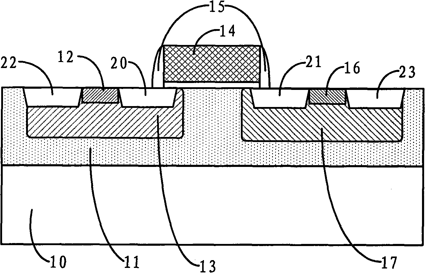
[0004] in such as figure 1 In the shown LDMOS device, its high-voltage well 11, source drift region 13 and drain drift region 17 are the base, emitter and collector of the parasitic BJT respectively; prior art ensures that the LDMOS device has a higher breakdown Voltage, the doping concentration of the high-voltage well 11 is low, which will lead to a large base resistance Rb of the parasitic BJT; and the base-emitter voltage Ube of the parasitic BJT is equal to the product of the base resistance Rb and the base current Ib, and the silicon material The base-emitter voltage Ube is a constant value of 0.7V. When the base-emitter voltage Ube is greater than 0.7V, the parasitic BJT is turned on and the LDMOS device is out of control, resulting in the rebound phenomenon of the LDMOS device at a lower voltage and the rebound performance Poor, which in turn reduces the maximum operating voltage of the LDMOS device
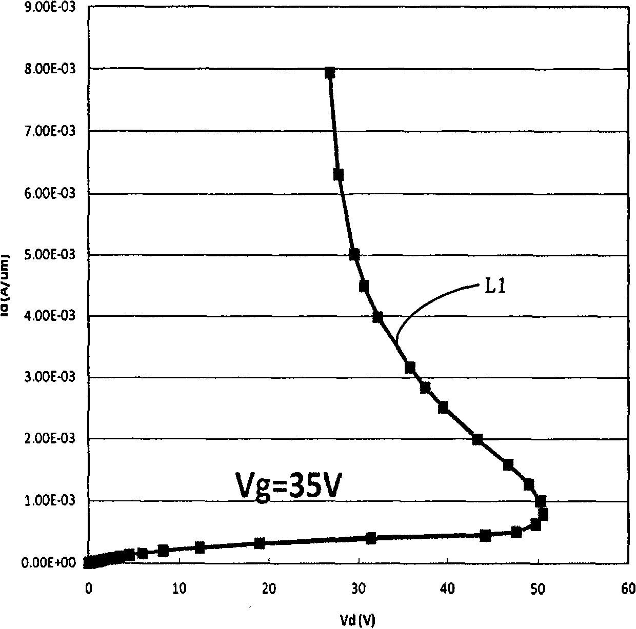
[0005] see figure 2 , which shows the Id-Vd relationship curve of the n-channel LDMOS device in the prior art when Vg is equal to 35V, as shown in the figure, the curve L1 is the Id-Vd relationship curve, and it can be seen from the curve L1 that the LDMOS device Id increases with the increase of Vd from the initial stage. When Vd increases to about 50V, the parasitic BJT corresponding to the LDMOS device is turned on and a bounce phenomenon occurs. In the prior art, the LDMOS device occurs at a lower drain voltage. Bounce back, resulting in poor bounce performance

Method used


Image

  • LDMOS device capable of improving rebound performance and manufacturing method thereof
  • LDMOS device capable of improving rebound performance and manufacturing method thereof
  • LDMOS device capable of improving rebound performance and manufacturing method thereof

Examples


Embodiment Construction

[0024] The LDMOS device capable of improving snapback performance and its manufacturing method of the present invention will be further described in detail below.

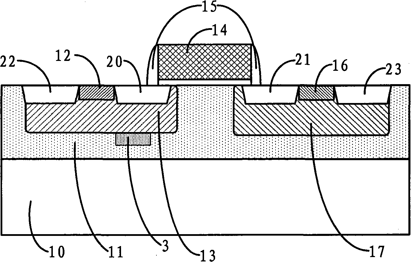
[0025] see image 3 , the LDMOS device of the present invention that can improve bounce performance includes a silicon substrate 10, a high voltage well 11, a source 12, a source drift region 13, a gate 14, a gate spacer 15, a drain 16, and a drain drift region 17. Near-gate trench isolation structures 20 and 21 , far-gate trench isolation structures 22 and 23 , and drag reducing block 3 . Each component of the LDMOS device capable of improving snapback performance of the present invention will be described in detail below.

[0026] The high voltage well 11 is formed in the silicon substrate 10, the source drift region 13 and the drain drift region 17 are formed in the high voltage well 11 and arranged on both sides of the gate 14, the source 12 and the drain 16 are respectively formed in the source drift region ...


PUM


Abstract

The invention discloses an LDMOS device capable of improving rebound performance and a manufacturing method thereof. In the prior art, the LDMOS device has poor rebound performance because a low doping concentration of a high-voltage trap needs to be maintained to ensure that the LDMOS device has a high breakdown voltage. The LDMOS device capable of improving the rebound performance of the invention comprises a silicon substrate, a high-voltage trap, a source, a source drift region, a drain, a drain drift region, a gate and a side wall thereof; the LDMOS device also comprises a relieving block which is arranged in the high-voltage trap and is adjacent to the source drift region; and the relieving block has the same doping type as the high-voltage trap and has a higher impurity concentration than the high-voltage trap. Due to the arrangement of the relieving block, the LDMOS device can effectively reduce the base resistance of a parasitic BJT in the LDMOS device without changing the impurity concentration of the high-voltage trap, thereby effectively improving the maximum working voltage of the LDMOS device and improving the rebound performance of the LDMOS device.

Description

technical field [0001] The invention relates to the field of semiconductor manufacturing, in particular to an LDMOS device capable of improving bounce performance and a manufacturing method thereof. Background technique [0002] Power MOS tubes are widely used in power electronic equipment. When they are forward biased, they are majority carrier conductive, and are usually regarded as devices that do not have secondary breakdown. However, the power MOS transistor has a parasitic bipolar transistor (BJT), and the collector and emitter of the parasitic BJT are also the drain and source of the MOS transistor. When there is a large drain current Id and a high drain voltage Vd at the drain of the power MOS transistor, the ionization in the device is intensified, and a large amount of hole current appears, which flows into the source through the base resistance Rb of the parasitic BJT, resulting in parasitic BJT The base potential Vb rises, and the so-called snapback phenomenon o...

Claims


Application Information

Patent Timeline
IPC IPC(8): H01L29/78H01L29/06H01L29/36H01L21/336
Inventor 王颢
Owner SHANGHAI HUAHONG GRACE SEMICON MFG CORP
Learn More