Deposition method capable of enhancing preferred orientation growth of AlN film
A technology of preferred orientation and deposition method, which is applied in the field of AlN thin film preparation process, can solve the problems of polluting AlN thin film, complicated process, and increased process cost, and achieve the effects of reducing surface roughness, simple process operation, and increasing propagation speed
- Summary
- Abstract
- Description
- Claims
- Application Information
AI Technical Summary
Problems solved by technology
Method used
Image
Examples
Embodiment 1
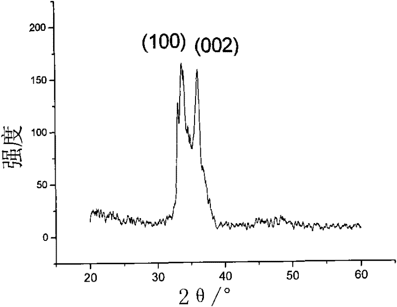
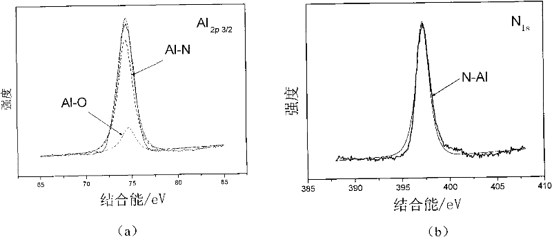
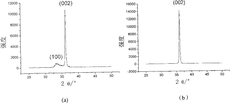
[0033] Example 1 Deposit (002) oriented AlN thin film on Si substrate: use (100) single crystal silicon wafer as substrate, successively wash with acetone and alcohol ultrasonically, dry and put into ion beam magnetron sputtering composite coating equipment in vacuum On the sample stage in the room, use 600eV / 50mA Ar before coating + The surface of the silicon wafer was cleaned by beam bombardment for 15 min. Ion beam assisted deposition of a homogeneous transition layer, that is, while sputtering an Al target with an ion beam, uses another beam of mid-energy N + The ion beam was used for auxiliary bombardment, and the specific process is shown in Table 2. After the transition layer was deposited, the sample stage was transferred from the ion beam coating position to the magnetron sputtering coating position through the rotating device without breaking the vacuum, and the process conditions were adjusted to the magnetron sputtering coating conditions. The AlN film was deposi...
Embodiment 2
[0043] Preparation of AlN thin film on embodiment 2 diamond substrate: in the application of surface acoustic wave device, diamond substrate has high acoustic velocity (18000m / s), the highest modulus of elasticity (1200GPa), does not need to reduce interdigitation The operating frequency of the device can be increased when the electrode width is reduced, so diamond is used as the substrate to prepare the AlN film.
[0044] Process flow: diamond substrate → acetone ultrasonic cleaning for ten minutes → alcohol ultrasonic cleaning for ten minutes → drying → loading on the sample stage in the vacuum chamber of the ion beam magnetron sputtering composite coating device (substrate temperature 500 ° C and rotating) → use 600eV, 50mA low energy Ar + Beam bombardment cleaning of silicon wafer surface for 15 minutes → ion beam assisted deposition of homogeneous transition layer (see Table 2 for specific process) → pulse reactive magnetron sputtering to deposit AlN thin film for 4 hours...
PUM
| Property | Measurement | Unit |
|---|---|---|
| surface roughness | aaaaa | aaaaa |
| surface roughness | aaaaa | aaaaa |
| surface roughness | aaaaa | aaaaa |
Abstract
Description
Claims
Application Information


