
Patsnap Eureka
For R&D, Patsnap Eureka makes reading and utilizing patents & technical documents easy.
Patsnap Eureka AIR
Designed for self-driven R&D workflows. Generate viable solutions, solve complex R&D challenges, empower your innovation with AI.

Patsnap Eureka Materials
Designed for material experts only. Revolutionize your material R&D, from search, analyze, to developing new materials.

TechResearch
Generate reliable direction feasibility study reports for your R&D in just a few steps.

TechSeek
Discover and master advanced knowledge NOW. Basics, ideas, possibilities, all at once.

TechMind
As an expert in R&D Theories, TechMind can generates customized viable solutions instantly.

TechRisk
Analyze your overall solution with one click, know your potential R&D risks in advance.

TechMonitor
Get weekly tech updates, stay abreast of the latest tech innovations and key insights.
Forming method of MOS (Metal Oxide Semiconductor) transistor and threshold voltage regulating method thereof
A technology of MOS transistors and threshold voltages, which is applied in the manufacture of circuits, electrical components, semiconductors/solid-state devices, etc., can solve problems such as the complexity of the MOS transistor manufacturing process, and achieve the effect of shortening the process cycle and saving costs
- Summary
- Abstract
- Description
- Claims
- Application Information
AI Technical Summary
Problems solved by technology
Method used
Image

Examples
Embodiment Construction
[0034] Although the invention will be described in more detail below with reference to the accompanying drawings, in which preferred embodiments of the invention are shown, it should be understood that those skilled in the art can modify the invention described herein and still achieve the advantageous effects of the invention. Therefore, the following description should be understood as a broad instruction for those skilled in the art, rather than as a limitation of the present invention.
[0035] In the following paragraphs the invention is described more specifically by way of example with reference to the accompanying drawings. Advantages and features of the present invention will become apparent from the following description and claims. It should be noted that the drawings are all in a very simplified form and use imprecise ratios, which are only used to facilitate and clearly assist the purpose of illustrating the embodiments of the present invention.
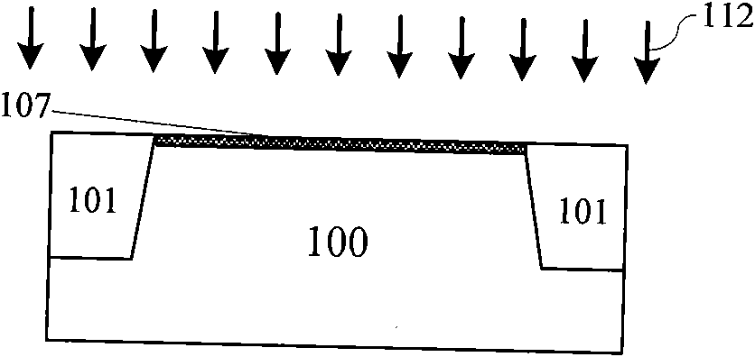
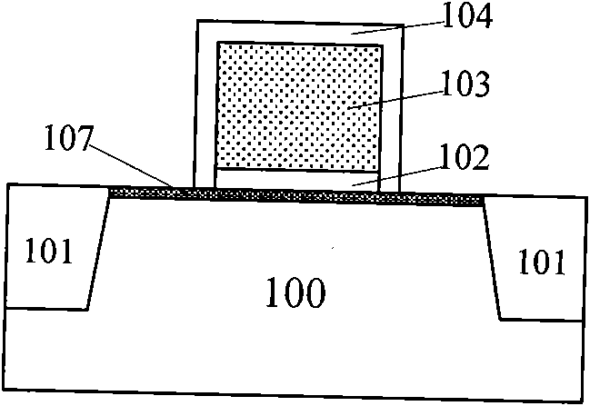
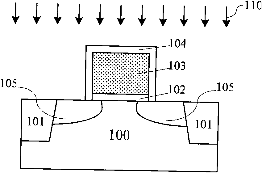
[0036] The step...
PUM
 Abstract
Description
Claims
Application Information
 - R&D Engineer
- R&D Manager
- IP Professional
- Industry Leading Data Capabilities
- Powerful AI technology
- Patent DNA Extraction
Browse by: Latest US Patents, China's latest patents, Technical Efficacy Thesaurus, Application Domain, Technology Topic, Popular Technical Reports.
© 2024 PatSnap. All rights reserved.Legal|Privacy policy|Modern Slavery Act Transparency Statement|Sitemap|About US| Contact US: help@patsnap.com