Visual inspection method for chip electronic component position error based on edge fitting

An electronic component and edge fitting technology, applied in the field of image processing, can solve the problems of slow detection speed, poor accuracy, and reduced efficiency, and achieve the effect of fast calculation speed

Inactive Publication Date: 2010-09-22
HOHAI UNIV CHANGZHOU
View PDF5 Cites 30 Cited by
  • Summary
  • Abstract
  • Description
  • Claims
  • Application Information

AI Technical Summary

Problems solved by technology

[0003] The purpose of the present invention is to overcome the defects of slow detection speed, poor precision and low efficiency of the position detection of chip electronic components in traditional chip mounters, and provide a visual detection method for position errors of chip electronic components based on edge fitting, which can be high-speed and accurate. , Reliably realize real-time detection of position error of chip electronic components

Method used


Image

  • Visual inspection method for chip electronic component position error based on edge fitting
  • Visual inspection method for chip electronic component position error based on edge fitting
  • Visual inspection method for chip electronic component position error based on edge fitting

Examples


Embodiment Construction

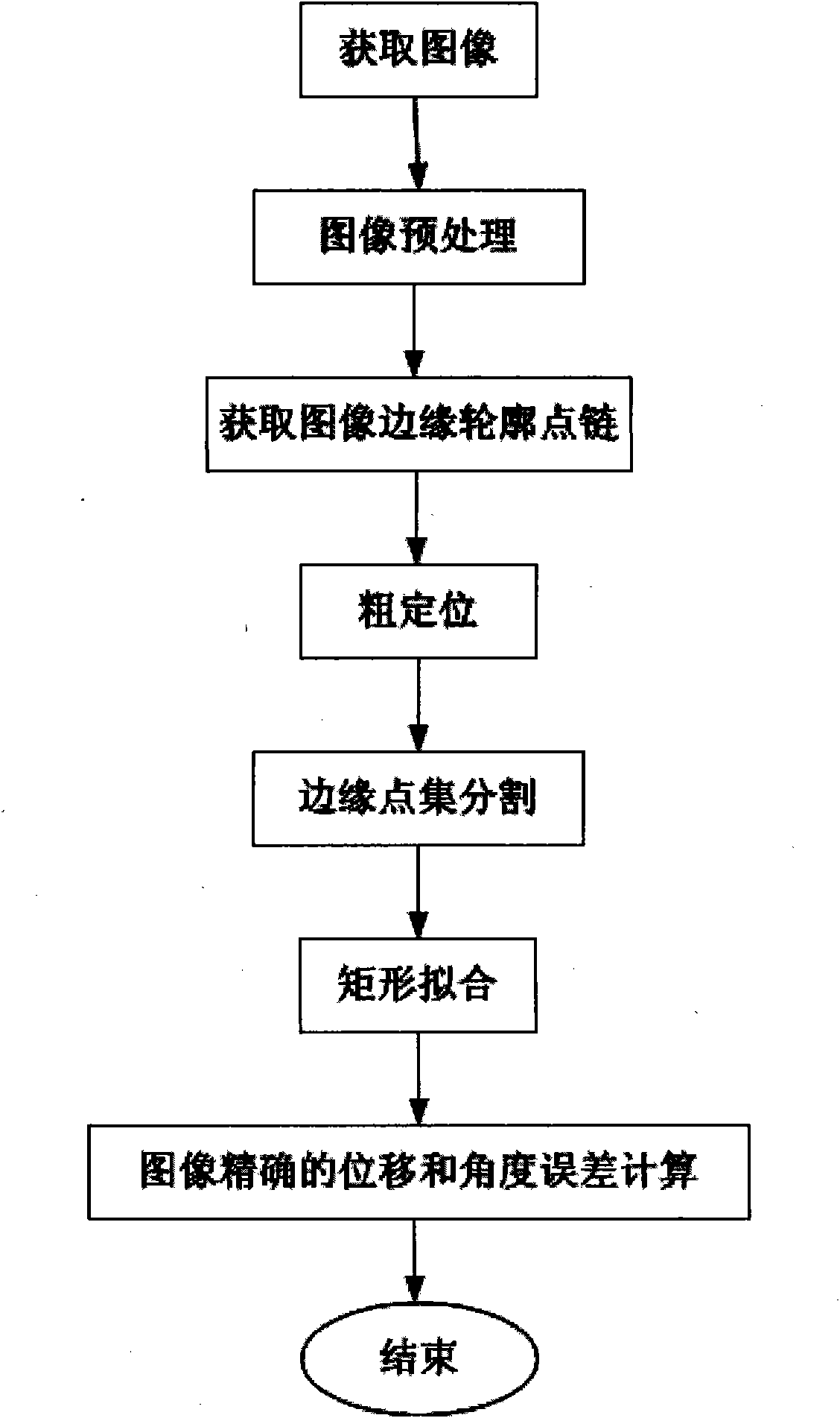
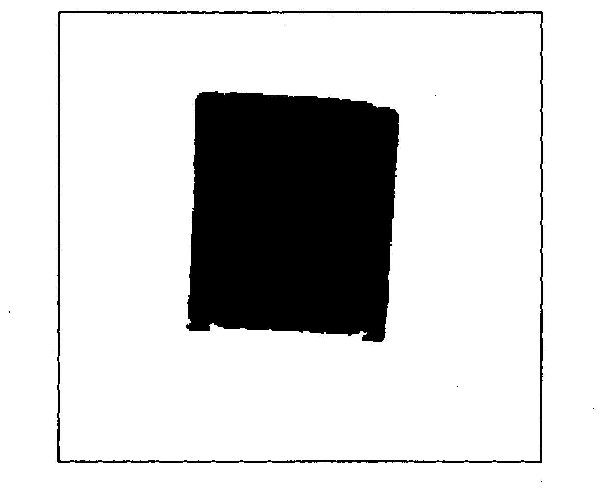
[0014] In the present invention, a general-purpose camera is first used to obtain a grayscale image of a chip electronic component, the image is preprocessed, and binarization is performed through threshold segmentation. After the binarization, the following is obtained: figure 2 image to isolate the target region. then to figure 2 The image after binary processing shown in the figure is subjected to edge detection and contour extraction at the same time. image 3 The edge contour of the image of the chip electronic component is shown, and then the boundary contour point set Ω of the entire image is obtained by boundary tracking, and the edge point chain structure of the image is generated.

[0015] Such as Figure 4 As shown, according to the obtained edge point chain structure, the center O(x c ,y c ) for preliminary calculation, the center coordinates of the contour (x c ,y c ) is calculated using the following contour center of gravity formula:

[0016] ...


PUM


Abstract

The invention discloses a visual inspection method for chip electronic component position error based on edge fitting. The method is that a boundary contour point set of an entire image is obtained by adopting boundary following to generate the edge point chain structure of the image; the image center a chip electronic component is preliminarily calculated by adopting a contour gravity center method, a corner is roughly calculated by adopting a closest-to-center point method, two lines which pass through the image center and are perpendicular to each other are established, the two lines divides the image contour into four areas containing corner points, four corner points are obtained in each area respectively according to the distance from a point to the center and four line sides are formed, and the corresponding edge point set is extracted by using the four line sides to partition an edge; and the edge fitting is conducted to each edge point set by adopting an edge point set rectangle least square method to obtain the fitting rectangle of the edge, and the center coordinates of the fitting rectangle and the corner relative to a horizontal direction are calculated. The invention has the advantages that the center position and the corner of the chip surface mounting component can be accurately inspected and the calculation speed is fast.

Description

technical field [0001] The invention belongs to the field of image processing used by the visual system of a placement machine in the surface mounting process of electronic components, in particular to the visual detection of position errors of chip electronic components. Background technique [0002] The rapid development of modern electronic technology requires the placement machine to develop in the direction of miniaturization, light weight, high integration and high reliability, that is, the product is required to be light, thin, short, small, good and economical. During the visual inspection of the placement machine used in the traditional surface mount process of electronic components, when using general-purpose cameras to capture images and visual processing software to detect the position of chip electronic components, due to the limitations of the general-purpose visual processing software itself, it is difficult According to the characteristics of chip electronic ...

Claims


Application Information

Patent Timeline
Patent Type & Authority Applications(China)
IPC IPC(8): G01B11/00G01B11/26G06T7/00G06T7/10G06T7/136G06T7/66
Inventor 朱灯林姜利何钢
Owner HOHAI UNIV CHANGZHOU
Why Eureka
Try Eureka