Phase compensation film
A phase compensation and film thickness technology, applied in optics, instruments, optical components, etc., can solve the problems of increasing cost, unable to complete dozens of layers of coating, restricting the development of optical technology, etc. Improve the quality of domestic optical instruments and the effect of mass production
- Summary
- Abstract
- Description
- Claims
- Application Information
AI Technical Summary
Problems solved by technology
Method used
Image

Examples
Embodiment Construction
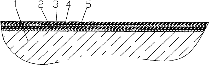
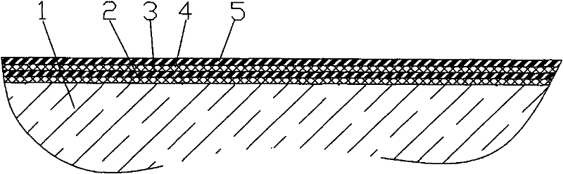
[0010] The accompanying drawing is a schematic diagram of the structure of the film layer of the present invention, as shown in the figure: the phase compensation film of this embodiment is plated through the steps of cleaning, vacuum evaporation and drying, and the film layer is sequentially outward from the optical substrate 1 including the first One layer of zirconia layer 2, the second layer of silicon oxide layer 3, the third layer of zirconia layer 4 and the fourth layer of silicon oxide layer 5; the thickness of the first layer of zirconia layer 2 is (transmittance maximum value-transmittance minimum value)×0.806+the minimum film thickness corresponding to the minimum transmittance value; the thickness of the second layer of silicon oxide layer 3 is the minimum film thickness corresponding to the minimum transmittance value+4.3nm; the third layer of zirconia layer The thickness of 4 is the minimum film thickness corresponding to the maximum value of transmittance × 0.822...
PUM
| Property | Measurement | Unit |
|---|---|---|
| reflectance | aaaaa | aaaaa |
| reflectance | aaaaa | aaaaa |
| reflectance | aaaaa | aaaaa |
Abstract
Description
Claims
Application Information