Data management method and flash memory storage system and controller using the same
A flash memory controller, data management technology, applied in memory systems, electrical digital data processing, instruments, etc., can solve problems such as delaying the operation of computer host systems
- Summary
- Abstract
- Description
- Claims
- Application Information
AI Technical Summary
Problems solved by technology
Method used
Image
Examples
no. 1 example
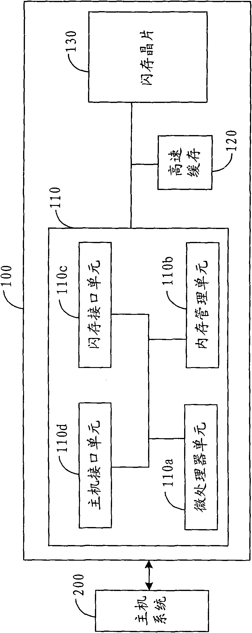
[0051] figure 1 is a schematic structural diagram of the flash memory storage system according to the first embodiment of the present invention.
[0052] Please refer to figure 1 , usually the flash storage system 100 will be used together with the host system 200 so that the host system 200 can write data into the flash storage system 100 or read data from the flash storage system 100 . In this embodiment, the flash storage system 100 is a solid state drive (SSD). But it must be understood that in another embodiment of the present invention, the flash memory storage system 100 can also be a memory card or a flash drive.
[0053] The flash storage system 100 includes a flash controller 110 , a cache 120 and a flash chip 130 .
[0054] The flash memory controller 110 executes a plurality of logic switches or control commands implemented in hardware or firmware, and writes, reads, and erases data in the flash memory chip 130 according to the instructions of the host system 20...
no. 2 example
[0091] Compared with the first embodiment, the second embodiment judges whether the time required to write all the temporarily stored write data in the physical unit will exceed the above-mentioned processing time upper limit based on the amount of temporarily stored data in the current cache, The flash memory storage system of the second embodiment judges whether the time required to write all the temporarily stored write data in the physical unit will exceed the above-mentioned processing time upper limit according to the dispersion degree of the write data temporarily stored in the cache. value. Here, the schematic diagram of the hardware structure of the second embodiment is similar to that of the first embodiment, and will be used below figure 1 , figure 2 , Figure 3A with 3C Now let's proceed to the description of the second embodiment.
[0092]Similar to the operation of the first embodiment, in this embodiment, when the host system 200 intends to write data to th...
no. 3 example
[0100] The difference between the third embodiment and the first embodiment is that the flash memory storage system according to the third embodiment judges whether the time required to write all the temporarily stored write data in the physical unit is Exceeded the processing time limit above. Here, the third embodiment is similar to the hardware structure diagram of the first embodiment, and the following will be figure 1 , figure 2 , Figure 3A-3C Now let's proceed to the description of the third embodiment.
[0101] Similar to the operation of the first embodiment, in this embodiment, when the host system 200 intends to write data to the flash memory storage system 100, the memory management unit 110b will receive a write command and a write data from the host system 200, Wherein the write command includes the logical address to store the write data. Afterwards, the memory management unit 110b converts the logical address into a corresponding logical unit, and tempora...
PUM
 Abstract
Description
Claims
Application Information


