
Static random access memory

A technology of static random access and memory, applied in the direction of static memory, digital memory information, information storage, etc., can solve the problems of unfavorable capacity expansion and layout and wiring of transistors, so as to facilitate capacity expansion and layout and wiring, save space, avoid The effect of read disturbance

Active Publication Date: 2010-11-03
SHANGHAI HUAHONG GRACE SEMICON MFG CORP
View PDF4 Cites 5 Cited by
  • Summary
  • Abstract
  • Description
  • Claims
  • Application Information

AI Technical Summary

Problems solved by technology

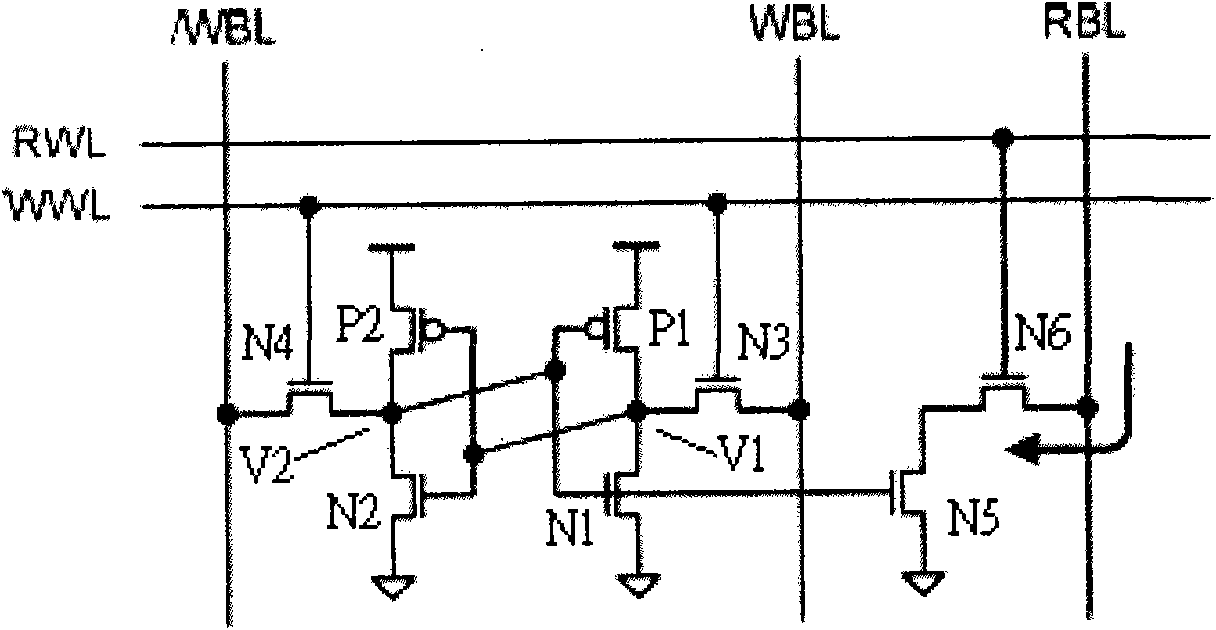
[0006] In order to overcome the shortcomings of read disturbance in the static random access memory of the prior art and the disadvantages of capacity expansion and layout and wiring caused by using more transistors to eliminate read disturbance, the main purpose of the present invention is to provide a static random access memory , which only uses six transistors and can eliminate the problem of read disturbance, which is conducive to capacity expansion and layout and wiring

Method used


Image

  • Static random access memory
  • Static random access memory
  • Static random access memory

Examples


Embodiment Construction

[0030] The implementation of the present invention is described below through specific examples and in conjunction with the accompanying drawings, and those skilled in the art can easily understand other advantages and effects of the present invention from the content disclosed in this specification. The present invention can also be implemented or applied through other different specific examples, and various modifications and changes can be made to the details in this specification based on different viewpoints and applications without departing from the spirit of the present invention.

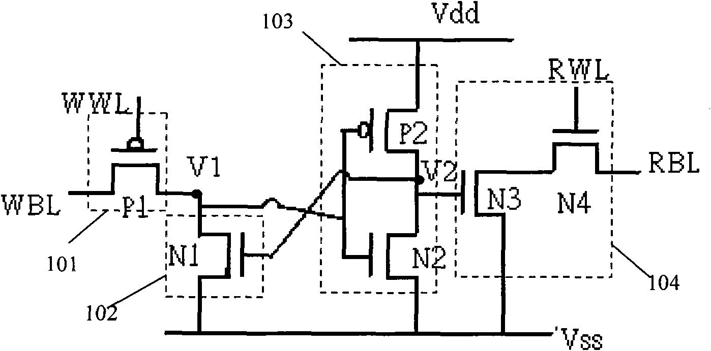
[0031] image 3 It is a circuit structure diagram of the first preferred embodiment of a six-transistor SRAM of the present invention. like image 3 As shown, a static random access memory of the present invention includes a write control circuit module 101 , a first reverse circuit 102 , a second reverse circuit 103 and a read buffer circuit 104 . The write control circuit module 101 is ...


PUM


Abstract

The invention discloses a static random access memory comprising a writing control circuit module, a first inverter circuit, a second inverter circuit and a reading buffer circuit, wherein the writing control circuit module is used for controlling the static random access memory; the first inverter circuit is coupled with the writing control circuit module to form a first storage node; the second inverter circuit is connected between a voltage source and a complementary voltage source; and the reading buffer circuit is coupled to a reading word line and a reading bit line and is coupled together with the first inverter circuit and the second inverter circuit to form a second storage node. The invention isolates the reading bit line from the second storage node by utilizing the reading buffer circuit and controls the state of information written by the static random access memory, thereby solving the problem of reading interference existing in the prior art.

Description

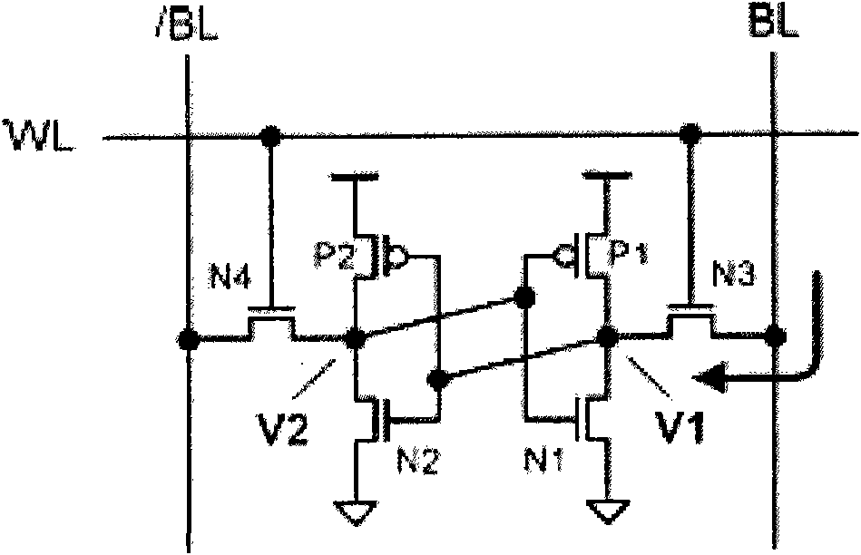
technical field [0001] The present invention relates to a semiconductor memory device, in particular to a static random access memory capable of eliminating read disturbance. Background technique [0002] Static Random Access Memory (SRAM) is often used in computer systems to temporarily store data. As long as there is continuous power supply, SRAM can maintain its stored state without any data update operation. An SRAM device includes an array of "cells," each of which can store a "bit" of data. A typical SRAM cell may include two cross-coupled inverters and two access transistors coupling the inverters to two complementary bit lines. Two access transistors are controlled by the word line to select the desired cell for a read or write operation. During a read operation, the access transistor is turned on to allow the charge remaining at the storage node of the cross-coupled inverter to be read through the bit line and the complementary bit line. During a write operation...

Claims


Application Information

Patent Timeline
Patent Type & Authority Applications(China)
IPC IPC(8): G11C11/413G11C11/419
Inventor 胡剑
Owner SHANGHAI HUAHONG GRACE SEMICON MFG CORP
Learn More