
Static random-access memory for eliminating reading interference

A technology of static randomness and read interference, which is applied in the direction of static memory, digital memory information, information storage, etc., can solve the problems of static random memory read interference, achieve the effect of avoiding read interference and improving stability

Active Publication Date: 2015-05-20
SHANGHAI HUAHONG GRACE SEMICON MFG CORP
View PDF5 Cites 0 Cited by
  • Summary
  • Abstract
  • Description
  • Claims
  • Application Information

AI Technical Summary

Problems solved by technology

[0004] The technical problem to be solved by the present invention is to provide a static random access memory, which solves the problem that the static random access memory is prone to read interference when reading

Method used


Image

  • Static random-access memory for eliminating reading interference
  • Static random-access memory for eliminating reading interference
  • Static random-access memory for eliminating reading interference

Examples


Embodiment Construction

[0013] The present invention will be further described in detail below in conjunction with the accompanying drawings and specific embodiments.

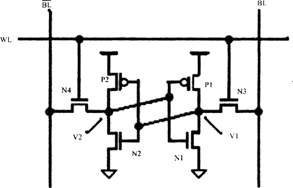
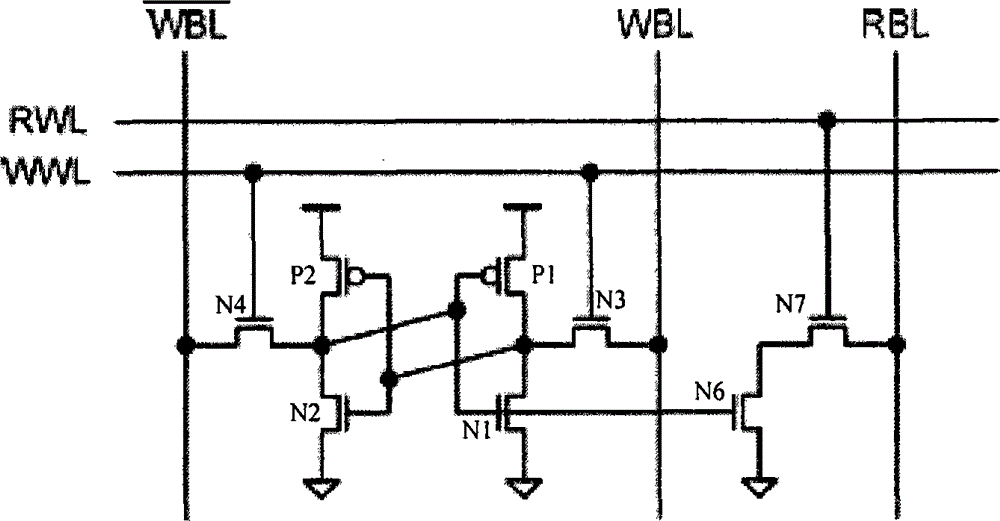
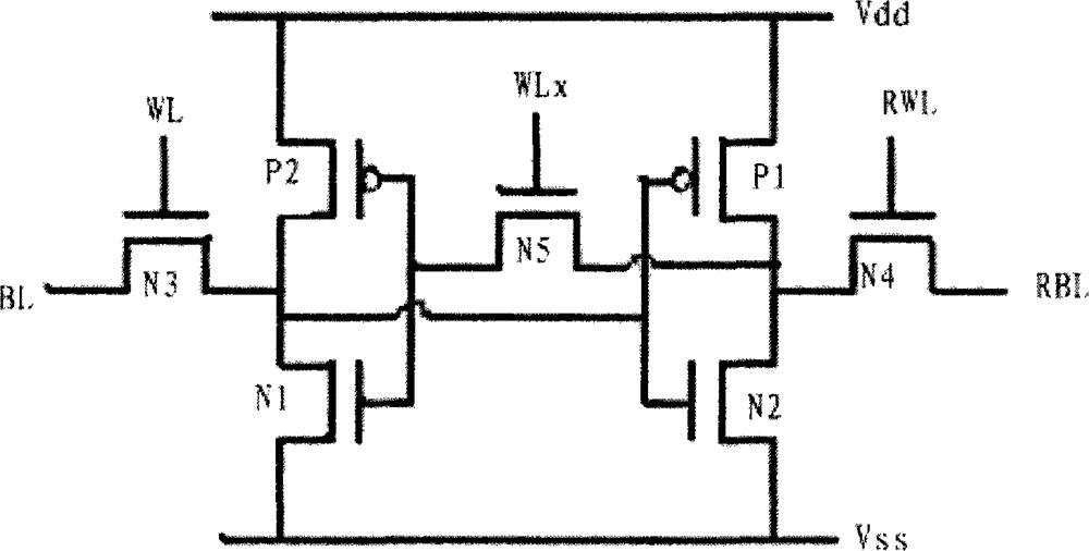
[0014] Please refer to image 3 , image 3 It is a static random access memory that eliminates read interference in the present invention. The static random access memory adds an NMOS transistor on the basis of the existing six-transistor static random access memory. The existing SRAM is composed of six transistors. The six transistors include four NMOS transistors (N1, N2, N3, N4) and two PMOS transistors (P1, P2), wherein the first PMOS transistor P1, the first NMOS transistor N1 and the second PMOS transistor P2, the first Two NMOS transistors N2 form two COMS inverters, and cross-coupling forms a bistable flip-flop; the third NMOS transistor N3 and the fourth NMOS transistor N4 of the gating transistor provide access and control for data input and output; in the figure BL, is a bit line control signal, WL is a word line of the ...


PUM


Abstract

The invention provides a static random-access memory for eliminating reading interference, which comprises a first NMOS tube, a second NMOS tube, a third NMOS tube, a fourth NMOS tube, a first PMOS tube, a second PMOS tube and a fifth NMOS tube. The first PMOS tube, the first NMOS tube, the second PMOS tube and the second NMOS tube forms two COMS phase reversers and form a flip and flop generator through cross-coupling; the third NMOS tube is connected with the second PMOS tube; the fourth NMOS tube is connected with the PMOS tube; and the fifth NMOS tube is respectively connected with the first PMOS tube and the second PMOS tube. The fifth NMOS tube is added in the static random-access memory, and the fifth NMOS tube is shut off when reading tasks are executed, so that the reading interference phenomenon is avoided, and the stability of the reading state of the static random-access memory is improved.

Description

technical field [0001] The invention relates to a semiconductor device, in particular to a static random access memory which eliminates read disturbance. Background technique [0002] The device density within an integrated circuit can be used to increase the performance of the integrated circuit and reduce its actual cost by using the principles of reduced geometry integrated circuit designs. Modern integrated circuit memory devices including Flash, SRAM (Static Random Access Memory), OUM, EEPROM, FRAM, MRAM, etc. are clear examples of utilizing this memory cell principle. Density within integrated circuit memory devices is continuing to increase, with a corresponding decrease in the unit memory cost of such devices. Increases in density are accomplished by making smaller structures within the device and by reducing the separation space between elements or structures that make up the elements. Usually, such smaller-sized design rules are accompanied by layout, design, and...

Claims


Application Information

Patent Timeline
Patent Type & Authority Patents(China)
IPC IPC(8): G11C11/4197
Inventor 胡剑
Owner SHANGHAI HUAHONG GRACE SEMICON MFG CORP
Learn More