
A stt-mram sensing circuit with good sensing margin

A sensing circuit and voltage sensor technology, applied in information storage, static memory, digital memory information, etc., can solve the problems that the circuit can no longer provide sensing reliability, high capacitance matching requirements, occupying a large area, etc., to achieve increased Large common-mode input range, increased sensing margin, and the effect of avoiding read disturbance

Active Publication Date: 2021-10-22
JIANGNAN UNIV
View PDF0 Cites 0 Cited by
  • Summary
  • Abstract
  • Description
  • Claims
  • Application Information

AI Technical Summary

Problems solved by technology

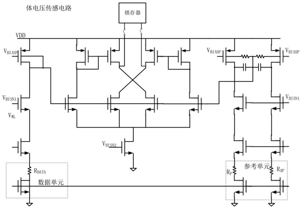
[0009] (1) As STT-MRAM scales to deep nano-nodes, VDD reduction between the two sensing branches and device mismatch issues (caused by PVT variations) increase, these circuits can no longer provide the required sensing reliability sex;
[0010] (2) Fixed reference voltage (V REF ) limits further reaching a larger sensing margin;
[0013] (1) Fixed reference voltage (V REF ) limits further reaching a larger sensing margin;
[0014] (2) The common-mode input range of the single-ended CMOS charge-transfer amplifier is small, so it limits the sensing data voltage (V DATA ) and reference voltage (V REF ) swing, and the input capacitive coupling method has high requirements for matching capacitance and will occupy a large area
[0015] Therefore, the above two methods cannot solve the RD and SM problems in STT-MRAM. In order to solve the RD and SM problems that exist when STT-MRAM extends to deep nano-nodes (for example, 40nm), a method with large SM and SM is required. Good sensing circuit for smaller RD

Method used


Image

  • A stt-mram sensing circuit with good sensing margin
  • A stt-mram sensing circuit with good sensing margin
  • A stt-mram sensing circuit with good sensing margin

Examples


Embodiment 1

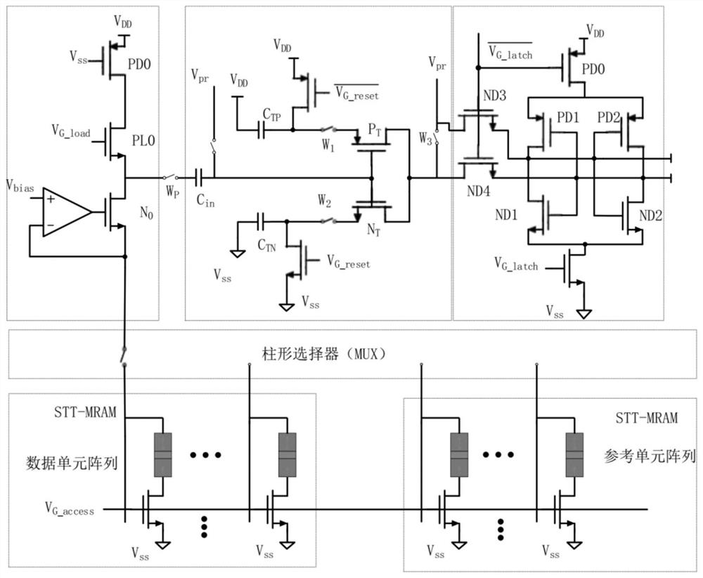
[0058] This embodiment provides a STT-MRAM sensing circuit with good sensing margin, see Figure 4 , the STT-MRAM sensing circuit includes: a voltage sensor, an amplifier and a dynamic latch voltage comparator; wherein, the voltage sensor includes a constant current source, a dynamic reference voltage generator, a voltage booster; the constant current source is fixed to read the current I read generates the bit line voltage V BL , bit line voltage V BL The sensing data voltage V is obtained through the booster DATA , while the bit line voltage V BL The dynamic reference voltage V is generated by the dynamic reference voltage generator REF , the amplifier uses a fully differential direct-coupled charge-transfer amplifier (CTA).

[0059] The circuit system measures the sensing data voltage (V DATA ) and reference voltage (V REF ), and then input these two voltages into a fully differential direct coupled charge transfer amplifier to output with then with Input to t...


PUM


Abstract

The invention discloses an STT-MRAM sensing circuit with good sensing margin, belonging to the technical field of computer storage. The STT-MRAM sensing circuit generates a dynamic reference voltage V by using a dynamic reference voltage generator REF , so that when the STT‑MRAM is in high impedance R AP , bit line voltage V BL_AP When larger, the dynamic reference voltage generator lowers the reference voltage, while when the STT‑MRAM is in low-impedance R P , bit line voltage V BL_P When it is small, the reference voltage is increased by the dynamic reference voltage generator, thereby greatly increasing |V REF -V DATA The value of |, thereby increasing the sensing margin SM; at the same time, using a constant current source will read the circuit I read Clamps in the 10‑100µA range to avoid read disturb (RD) during sensing operations.

Description

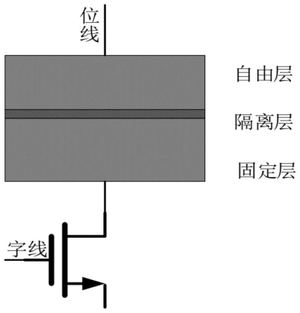
technical field [0001] The invention relates to an STT-MRAM sensing circuit with good sensing margin, belonging to the technical field of computer storage. Background technique [0002] Spin-torque magnetic random-access memory (STT-MRAM) has demonstrated great potential as a next-generation nonvolatile memory technology due to its zero standby power, high density, radiation hardness, and excellent scalability, etc. It has attracted extensive attention and research and development. A common STT-MRAM consists of a magnetic tunnel junction (MTJ) and an NMOS transistor. Among them, MTJ is used as a storage element, and it is accessed through an NMOS tube. The top-down isolation layer of MTJ can be divided into three layers: free layer, isolation layer and fixed layer. The free layer and the fixed layer are generally composed of ferromagnetic materials, while the middle isolation layer is composed of a very thin oxide, such as figure 1 shown. The magnetization direction of ...

Claims


Application Information

Patent Timeline
Patent Type & Authority Patents(China)
IPC IPC(8): G11C11/16G11C7/06G11C7/08
CPCG11C7/062G11C7/08G11C11/1673
Inventor 姜岩峰成关壹于平平梁海莲张曙斌
Owner JIANGNAN UNIV
Learn More