Supercharge Your Innovation With Domain-Expert AI Agents!

Reliable contact

A contact and active area technology, applied in the field of improved formation of nickel-based germanide contact, can solve problems such as disadvantage and high annealing temperature

Inactive Publication Date: 2010-11-24
AGENCY FOR SCI TECH & RES
View PDF0 Cites 0 Cited by
  • Summary
  • Abstract
  • Description
  • Claims
  • Application Information

AI Technical Summary

Problems solved by technology

This is because relatively high annealing temperatures are required to form titanium or cobalt junctions with good electrical properties such as low resistance, which is not good for germanium-based applications

Method used


Image

  • Reliable contact
  • Reliable contact
  • Reliable contact

Examples


Embodiment Construction

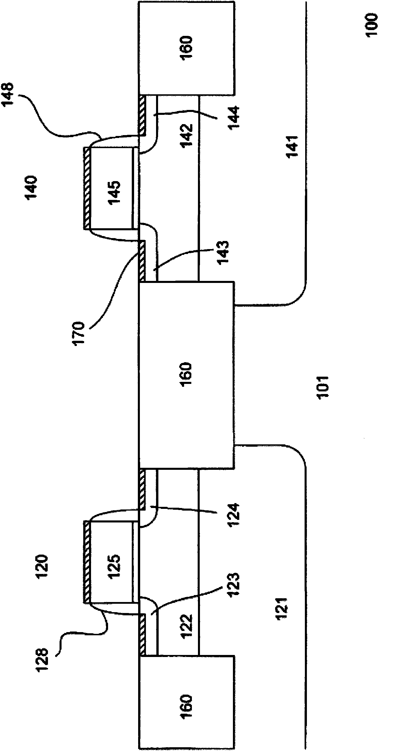
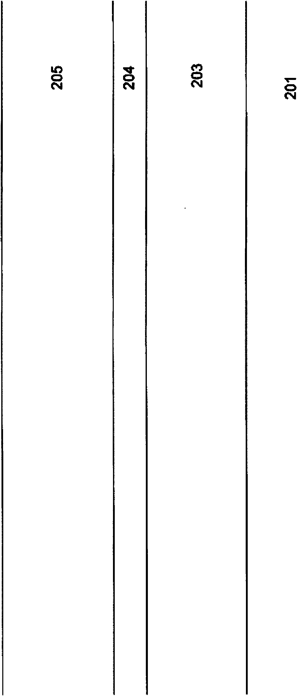
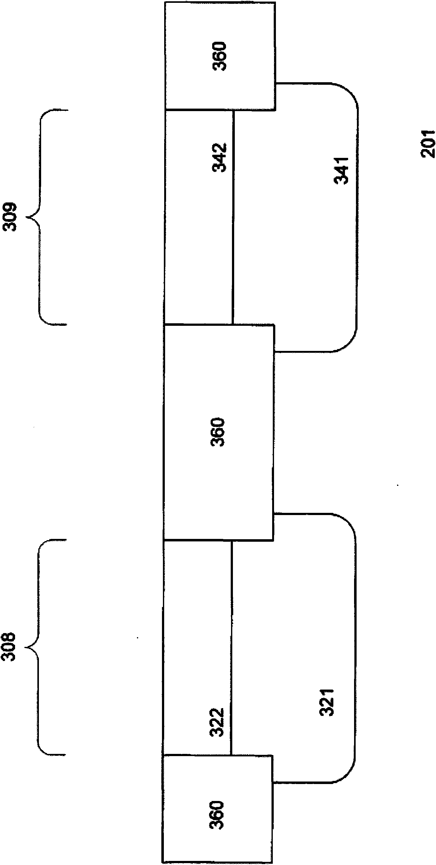
[0011] Figure 2-6 A process for forming a nickel-based contact according to one embodiment of the present invention is shown. refer to figure 2 , shows a cross-section of a portion of the substrate 201 . The substrate is used to form integrated circuit packages. In one embodiment, the substrate comprises a multilayer substrate in which at least the top or surface layer comprises germanium. For example, multilayer substrates include germanium-on-insulator substrates. The germanium-on-insulator substrate may comprise a silicon substrate substrate 203 having a top layer 205 comprising germanium separated by an insulator layer 204 such as silicon dioxide. The top layer of the substrate comprises, for example, single crystalline material, polycrystalline or amorphous material, or combinations thereof. The germanium layer can be tensioned or relaxed. A surface comprising germanium may also be provided on the silicon germanium substrate layer.

[0012] In another embodiment,...


PUM


Abstract

The invention discloses a nickel based germanide contact which comprises a processing material, wherein the processing material inhibits nickel based germanide from agglutinating in the process of forming the contact and the processes after the germaniding process. The processing material, which exists or is combined in the nickel layer used for forming a nick based contact in a mode of a covering layer on a nickel layer; and since agglutination is reduced, the electrical characteristic of the contact is improved.

Description

[0001] The present invention generally relates to the formation of germanide contacts for use in integrated circuits (ICs). More particularly, the invention relates to the improved formation of nickel-germanide contacts for use in integrated circuits. Background technique [0002] figure 1 A portion 100 of a conventional CMOS IC is represented. This part includes first and second complementary transistors 120 and 140 formed on a silicon substrate 101 . The first transistor is an n-MOS transistor formed on the deep p-doped well 121 , while the second transistor is a p-MOS transistor formed on the deep n-doped well 141 . The shallow p-doped well 122 is under the n-MOS transistor, while the shallow n-doped well is under the p-MOS transistor 142 . Shallow trench isolations 160 are used to isolate transistors. Each transistor includes a source electrode (123 or 143), a drain electrode (124 or 144), and a gate electrode (125 or 145). For n-MOS transistors, the source, drain and...

Claims


Application Information

Patent Timeline
IPC IPC(8): H01L23/485
CPCH01L21/28518
Inventor 池东植李家耀李德宝刘晓丽姚海标
Owner AGENCY FOR SCI TECH & RES
Features
  • R&D
  • Intellectual Property
  • Life Sciences
  • Materials
  • Tech Scout
  • Unparalleled Data Quality
  • Higher Quality Content
  • 60% Fewer Hallucinations
Learn More