Germanium-containing dielectric barrier for low-k process

a dielectric barrier and germanium-containing technology, applied in the direction of semiconductor devices, electrical equipment, semiconductor/solid-state device details, etc., can solve the problems of low-k dielectric layer stability, copper diffusion, and failure of conventional formation process of barrier layer, so as to reduce damage to low-k dielectric layer, reduce copper diffusion, and stabilize the effect of dielectric layer

Active Publication Date: 2008-06-12
TAIWAN SEMICON MFG CO LTD
View PDF6 Cites 13 Cited by
  • Summary
  • Abstract
  • Description
  • Claims
  • Application Information

AI Technical Summary

Benefits of technology

[0012]The advantageous features of the present invention include more stable dielectric layers, hence reduced copper diffusion, reduced damaged to low-k dielectric layers, and reduced resistivity of un-nitrided silicide layer.

Problems solved by technology

However, copper suffers from electro-migration (EM) and stress-migration (SM) reliability issues, particularly as geometries continue to shrink and current densities continue to increase.
The conventional formation process of barrier layers suffers drawbacks.
Since copper silicide is relatively unstable, silicon may still break from copper silicide and diffuse into low-k dielectric layer 2.
However, plasma treatments have the side effect of incurring damage to low-k dielectric layer 2. FIG. 2 schematically illustrates damaged low-k dielectric layers 8, which are damaged portions of low-k dielectric layer 2 adjacent copper line 4.
It is difficult to control the formation of copper silicide nitride layer without incurring the side effects.

Method used


Image

  • Germanium-containing dielectric barrier for low-k process
  • Germanium-containing dielectric barrier for low-k process
  • Germanium-containing dielectric barrier for low-k process

Examples


Embodiment Construction

[0018]The making and using of the presently preferred embodiments are discussed in detail below. It should be appreciated, however, that the present invention provides many applicable inventive concepts that can be embodied in a wide variety of specific contexts. The specific embodiments discussed are merely illustrative of specific ways to make and use the invention, and do not limit the scope of the invention.

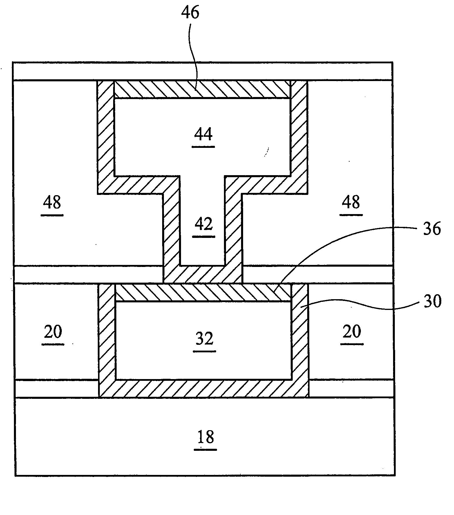
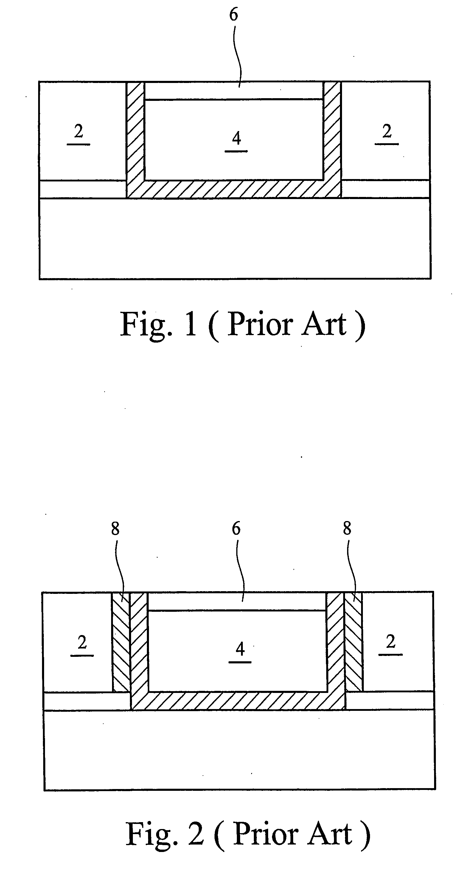
[0019]Interconnect structures comprising copper germanide nitride barrier layers and methods of forming the same are provided. The intermediate stages of manufacturing preferred embodiments of the present invention are illustrated in FIGS. 3 through 7. Throughout the various views and illustrative embodiments of the present invention, like reference numbers are used to designate like elements.

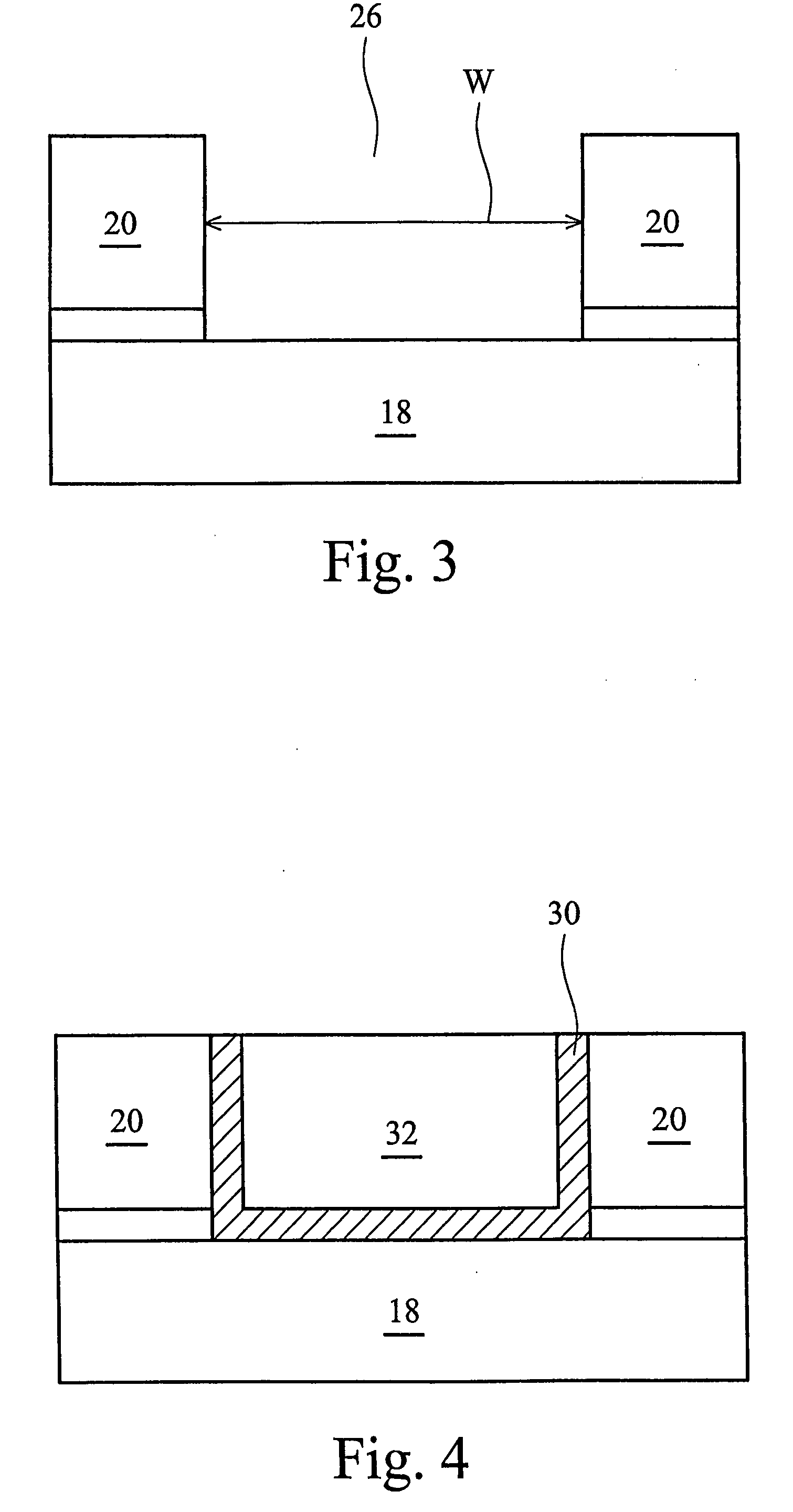
[0020]FIG. 3 illustrates the formation of opening 26 in dielectric layer 20, which is formed over a schematically illustrated base layer 18. Base layer 18 may include a semiconductor sub...


PUM

PropertyMeasurementUnit
dielectric constantaaaaaaaaaa
temperatureaaaaaaaaaa
pressureaaaaaaaaaa

Abstract

A semiconductor structure and methods of forming the same are provided. The semiconductor structure includes a semiconductor substrate; a first dielectric layer over the semiconductor substrate; a conductive wiring in the first dielectric layer; and a copper germanide nitride layer over the conductive wiring.

Description

CROSS REFERENCES[0001]This application claims the benefit of the following provisionally filed U.S. Patent application: Application Ser. No. 60 / 873,195, filed Dec. 6, 2006, entitled “Germanium-Containing Dielectric Barrier for Low-K Process,” which patent application is incorporated herein by reference.TECHNICAL FIELD[0002]This invention is related generally to integrated circuits, and more particularly to the structure and formation methods of interconnect structures in integrated circuits, and even more particularly to the formation of barrier layers on copper features.BACKGROUND[0003]A commonly used method for forming metal lines and vias is known as “damascene.” Generally, this method involves forming an opening in a dielectric layer, which separates the vertically spaced metallization layers. The opening is typically formed using conventional lithographic and etching techniques. After the formation, the opening is filled with copper or copper alloys to form a via or a trench. E...

Claims


Application Information

Patent Timeline
Patent Type & Authority Applications(United States)
IPC IPC(8): H01L23/52H01L21/3205
CPCH01L21/76834H01L21/76835H01L21/76849H01L21/76856H01L21/76867H01L21/76886H01L2924/0002H01L23/53238H01L23/53295H01L2924/00
Inventor LIU, CHUNG-SHIYU, CHEN-HUA
Owner TAIWAN SEMICON MFG CO LTD
Why Eureka
Try Eureka