Heat-treating methods and systems

a heat treatment and workpiece technology, applied in the field of objects heat treatment, can solve the problems of inability to heat treat workpieces, and high temperatures required to anneal the device side of semiconductor wafers, etc., to achieve the effect of reducing the magnitude of thermal gradients, and enhancing the cooling of the workpi

Inactive Publication Date: 2005-09-06
MATTSON TECHNOLOGY +1
View PDF92 Cites 63 Cited by
  • Summary
  • Abstract
  • Description
  • Claims
  • Application Information

AI Technical Summary

Benefits of technology

[0018]The present invention addresses the above needs by providing, in accordance with one aspect of the invention, a method and system for heat-treating a workpiece. The method includes pre-heating the workpiece to an intermediate temperature, heating a surface of the workpiece to a desired temperature greater than the intermediate temperature, and enhancing cooling of the workpiece. Pre-heating the workpiece to the intermediate temperature, prior to heating the surface to the higher desired temperature, decreases the magnitude of the thermal gradients that occur in the workpiece when the surface is heated to the desired temperature. Therefore, thermal stress in the workpiece is reduced. Where the workpiece has a crystal lattice structure, such as a semiconductor wafer for example, damage to the lattice is correspondingly reduced.
[0019]In addition, heating the surface of the workpiece to the desired temperature, as opposed to heating the entire workpiece to the desired temperature, results in much faster cooling of the surface, as the comparatively colder bulk or body of the workpiece may act as a heat sink to cool the surface by conduction. Where the workpiece is a dopant-implanted semiconductor wafer for example, this faster cooling results in shallower dopant diffusion, allowing for the formation of shallower junctions in accordance with modern and future industry requirements.
[0020]Enhancing cooling of the workpiece further reduces the time that the workpiece spends at high temperatures. In embodiments where the workpiece is a semiconductor wafer, this faster cooling again reduces dopant diffusion in the workpiece, allowing for the formation of shallower junctions.

Problems solved by technology

The ion implantation process damages the crystal lattice structure of the surface region of the wafer, and leaves the implanted dopant atoms in interstitial sites where they are electrically inactive.
The high temperatures required to anneal the device side of a semiconductor wafer tend to produce undesirable effects using existing technologies.
As performance demands of semiconductor wafers increase and device sizes decrease, it is necessary to produce increasingly shallow and abruptly defined junctions, and therefore, diffusion depths that would have been considered negligible in the past or that are tolerable today will no longer be tolerable in the next few years or thereafter.
Existing annealing technologies are generally incapable of achieving such shallow junction depths.
However, the wafer tends to remain hot for a considerable time after the power supply to the tungsten filaments is shut off, for a number of reasons.
Accordingly, if the wafer is heated with such a system to a sufficiently high temperature to repair the crystal lattice structure and activate the dopants, the wafer tends to remain too hot for too long a period of time, resulting in diffusion of the dopants to significantly greater depths in the wafer than the maximum tolerable diffusion depths that will be required to produce 30 nm junction depths.
Although the vast majority of dopant diffusion occurs in the highest temperature range of the annealing cycle, lowering the annealing temperature is not a satisfactory solution to the diffusion problem, as lower annealing temperatures result in significantly less activation of the dopants and therefore higher sheet resistance of the wafer, which would exceed current and / or future tolerable sheet resistance limits for advanced processing devices.
Thus, the wafer does not remain hot long enough for much dopant diffusion to occur.
However, because the bulk regions of the wafer, as well as device side areas other than the localized area heated by the laser, remain cold when the localized surface area of the device side is heated to annealing temperature, extreme thermal gradients are produced in the wafer, resulting in large mechanical strains which cause the crystal planes within the wafer to slip, thereby damaging or breaking the crystal lattice.
In this regard, a very small spatial movement may completely destroy the crystal lattice.
Thermal gradients may also cause other damage, such as warpage or defect generation.
Even in the absence of slippage, a non-uniform temperature distribution across the wafer may cause non-uniform performance-related characteristics, resulting in either inadequate performance of the particular wafer, or undesirable performance differences from wafer to wafer.
In addition, the large amount of energy delivered by the laser or lasers to the device side of the wafer is non-uniformly absorbed by the pattern of devices thereon, resulting in deleterious heating effects in regions of the wafer where annealing is not desired, and may also produce further large temperature gradients causing additional damage to the silicon lattice.
A typical temperature-time profile of the device side surface using this method is flat for a very long time, followed by a rapid increase and rapid cooling of the surface resulting from the laser anneal.
Although this method purports to reduce junction leakage currents as compared to laser annealing alone, the long duration of the low-temperature annealing stage causes the dopants to diffuse to greater depths within the device side of the wafer.
Such diffusion, which may have been tolerable or perhaps even negligible by early 1990s standards, would not permit the formation of sufficiently shallow junctions to comply with current performance and industry roadmap requirements.
In addition, as the substrate side is irradiated rather than the device side, non-uniform heating of the device side due to non-uniform absorption by the pattern of devices is also much lower than for laser annealing, resulting in lower lateral temperature gradients and reduced damage to devices.
However, early indications suggest that embodiments of this method may result in somewhat deeper diffusion of the dopants than laser annealing.
This caused the wafer to spend longer times at high temperatures, thereby tending to increase dopant diffusion to depths that would be unacceptable by modern standards.
In addition, the re-reflections of such radiation back to the wafer tended to produce non-uniform heating in the wafer, resulting in slippage and other problems associated with non-uniform or excessive heating.
Moreover, this method purported to be suitable for heating the wafer with 2% uniformity, which is not acceptable for modern RTP systems.
In addition, this method typically involved a delay of a few seconds between the isothermal heating stage and the subsequent thermal flux heating stage, during which the wafer remained at a relatively high intermediate temperature, such as 1100° C., for example.
This delay at the intermediate temperature can cause significant dopant diffusion, thus interfering with the ability to produce shallow junctions in accordance with modern performance requirements.

Method used


Image

  • Heat-treating methods and systems
  • Heat-treating methods and systems
  • Heat-treating methods and systems

Examples


first embodiment

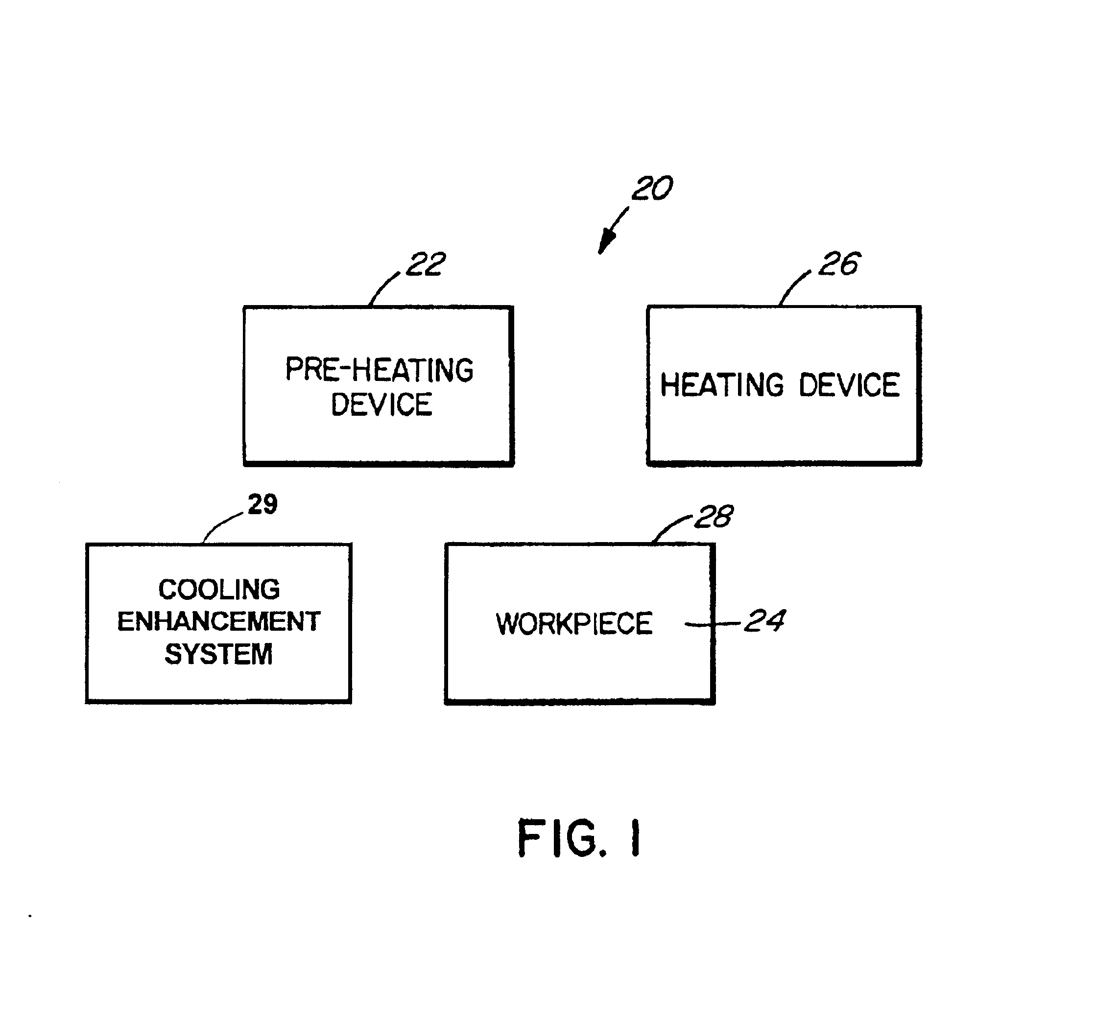
[0101]Referring to FIG. 1, a system for heat-treating a workpiece according to the invention is shown generally at 20. The system includes a pre-heating device 22 operable to pre-heat the workpiece 24 to an intermediate temperature, and a heating device 26 operable to heat a surface 28 of the workpiece to a desired temperature greater than the intermediate temperature. The system further includes a cooling enhancement system 29 for enhancing cooling of the workpiece to a temperature below the intermediate temperature.

System

second embodiment

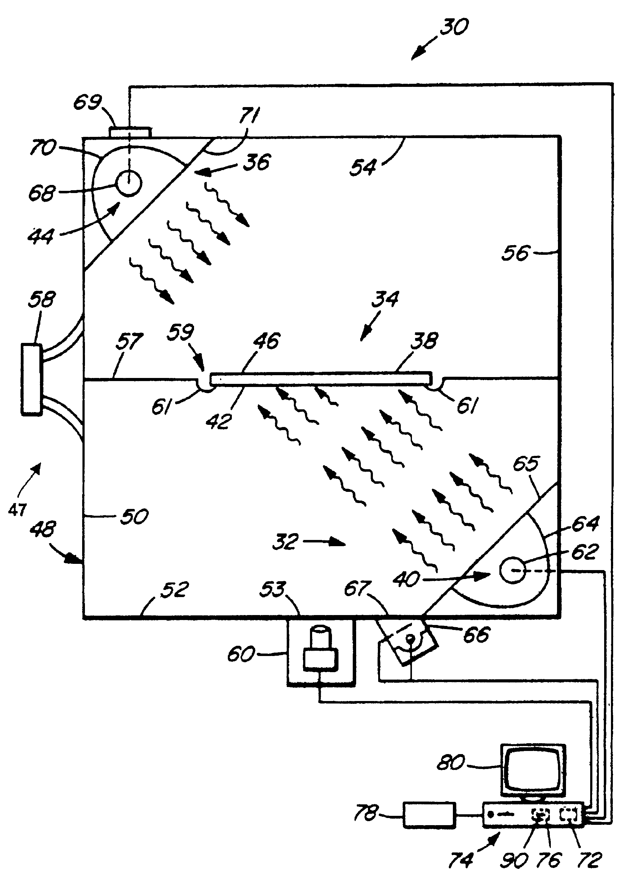
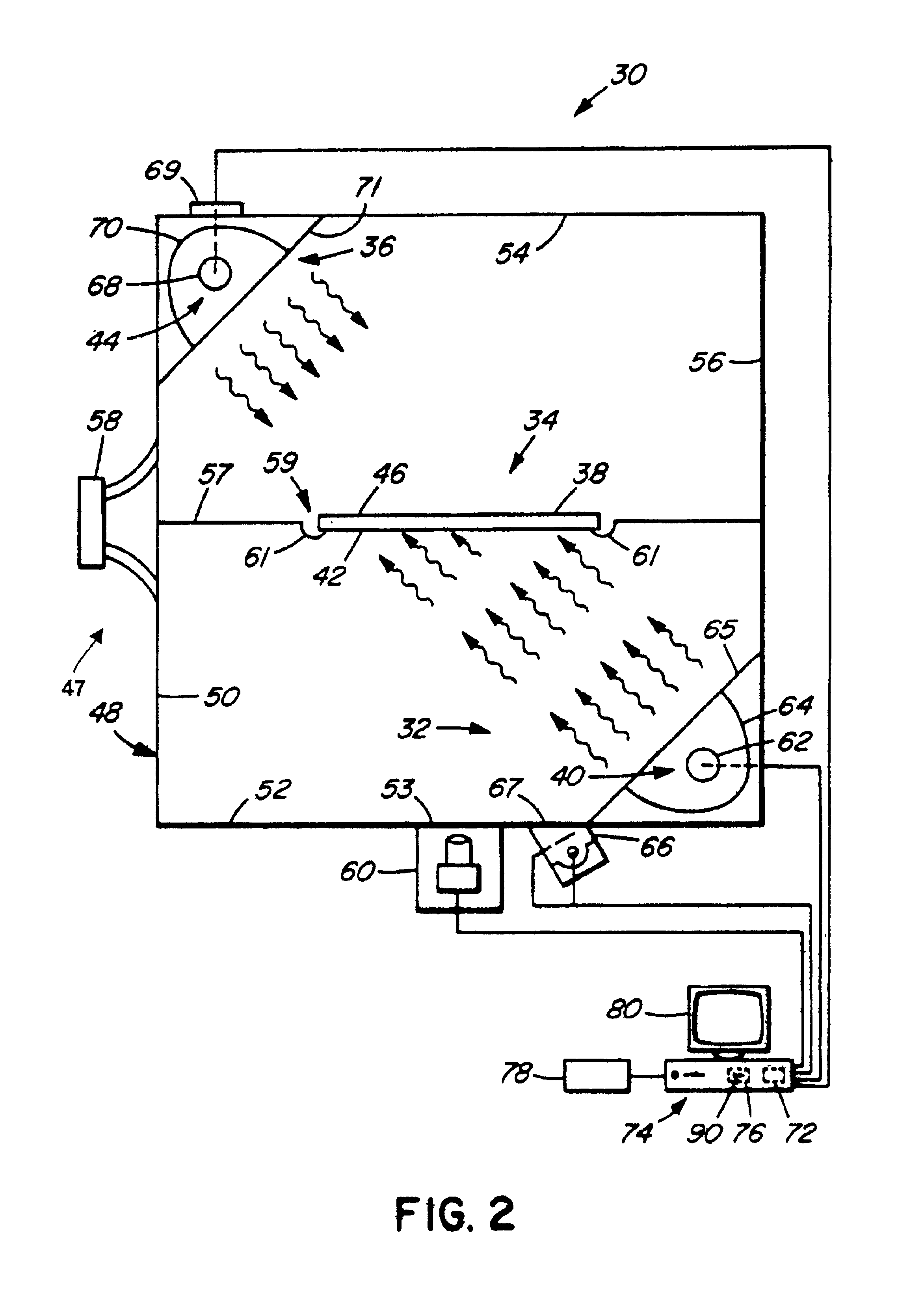
[0102]Referring to FIG. 2, a system for heat-treating a workpiece according to the invention is shown generally at 30. The system 30 includes a pre-heating device 32, operable to pre-heat a workpiece 34, which in this embodiment is a semiconductor wafer, to an intermediate temperature. The system further includes a heating device 36, which in this embodiment is operable to heat a surface 38 of the workpiece 34 to desired temperature greater than the intermediate temperature.

[0103]In this embodiment, the pre-heating device 32 is operable to pre-heat the workpiece 34 from an initial temperature to the intermediate temperature, and the heating device 36 is operable to heat the surface 38 of the workpiece 34 to the desired temperature, which is greater than the intermediate temperature by an amount less than or equal to about the difference between the intermediate and initial temperatures. In other words, a significant portion of the heating occurs during the heating from the initial t...

third embodiment

[0162]For example, referring to FIGS. 2 and 5, a system for heat-treating a workpiece according to the invention is shown generally at 200 in FIG. 5. In this embodiment, the pre-heating device 32 includes an alternative irradiance source, which in this embodiment includes at least one filament lamp. Thus, in this embodiment, irradiating the workpiece includes exposing the workpiece to electromagnetic radiation produced by at least one filament lamp. More particularly, in this embodiment the pre-heating device 32 includes a disc-shaped array 202 of tungsten filament lamps operable to project electromagnetic radiation through a quartz window 204 to irradiate the first side 42 of the workpiece 34, to pre-heat the workpiece to the intermediate temperature. Although there are numerous advantages to using an arc lamp rather than a tungsten filament lamp array as the pre-heating device 32, as discussed earlier herein, the deeper dopant diffusion that tends to result from tungsten filament ...


PUM

PropertyMeasurementUnit
temperatureaaaaaaaaaa
angleaaaaaaaaaa

Abstract

A method involves pre-heating a workpiece to an intermediate temperature, heating a surface of the workpiece to a desired temperature greater than the intermediate temperature, and enhancing cooling of the workpiece. Enhancing cooling may involve absorbing radiation thermally emitted by the workpiece. An apparatus includes a first heating source for heating a first surface of a semiconductor wafer, a second heating source for heating a second surface of the semiconductor wafer, and a first cooled window disposed between the first heating source and the semiconductor wafer.

Description

CROSS-REFERENCE TO RELATED APPLICATIONS[0001]This application is a continuation-in-part of U.S. patent application Ser. No. 09 / 729,747, filed Dec. 4, 2000, which is hereby incorporated herein by reference. This application further claims priority from Patent Cooperation Treaty application serial number PCT / CA01 / 00776, filed May 30, 2001, also incorporated herein by reference.FIELD OF THE INVENTION[0002]The present invention relates to heating of objects, and more particularly to methods and systems for heat-treating a workpiece.BACKGROUND OF THE INVENTION[0003]Many applications require heating or annealing of an object or workpiece. For example, in the manufacture of semiconductor chips such as microprocessors, a semiconductor wafer, such as a silicon wafer, is subjected to an ion implantation process, which introduces impurity atoms or dopants into a surface region of a device side of the wafer. The ion implantation process damages the crystal lattice structure of the surface regio...

Claims


Application Information

Patent Timeline
Patent Type & Authority Patents(United States)
IPC IPC(8): C30B31/00C30B31/12F27D19/00H01L21/02H01L21/00H01L21/268H01L21/324F27D23/00H01L21/265F27D99/00H01L21/26
CPCC30B31/12F27D19/00H01L21/268H01L21/2686H01L21/324H01L21/67115F27D2019/0003F27D2099/0026Y10S438/928
Inventor CAMM, DAVID MALCOLMELLIOTT, J. KIEFER
Owner MATTSON TECHNOLOGY
Why Eureka
Try Eureka