Method of forming self-aligned low resistance contact layer

a low-resistance contact layer and self-aligning technology, applied in the field of semiconductor processing, can solve the problems of high junction leakage, increase in the number, and deactivation of dopan

Active Publication Date: 2010-02-11
INTEL CORP
View PDF7 Cites 11 Cited by
  • Summary
  • Abstract
  • Description
  • Claims
  • Application Information

AI Technical Summary

Problems solved by technology

Furthermore, possible recessing of the substrate 100 due to excessive consumption by the metal layer 180 causes high junction leakage.
A two step annealing process

Method used


Image

  • Method of forming self-aligned low resistance contact layer
  • Method of forming self-aligned low resistance contact layer
  • Method of forming self-aligned low resistance contact layer

Examples


Embodiment Construction

[0010]A method of forming self-aligned low resistance contact layers is described. In the following description, numerous specific details are set forth in order to provide a thorough understanding of the present invention. In other instances, well known semiconductor processing techniques and features have not been described in particular detail in order not to unnecessarily obscure the present invention.

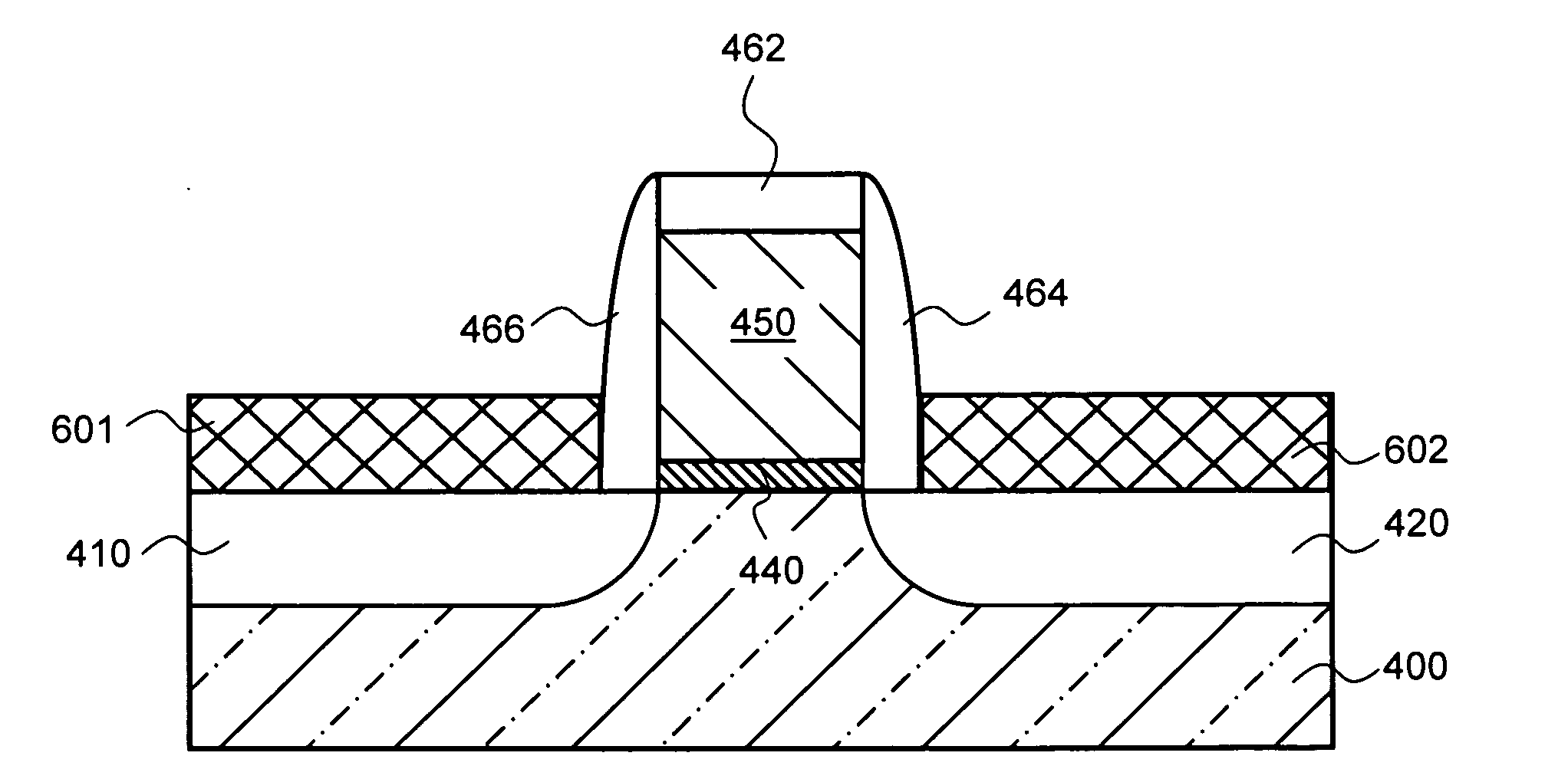
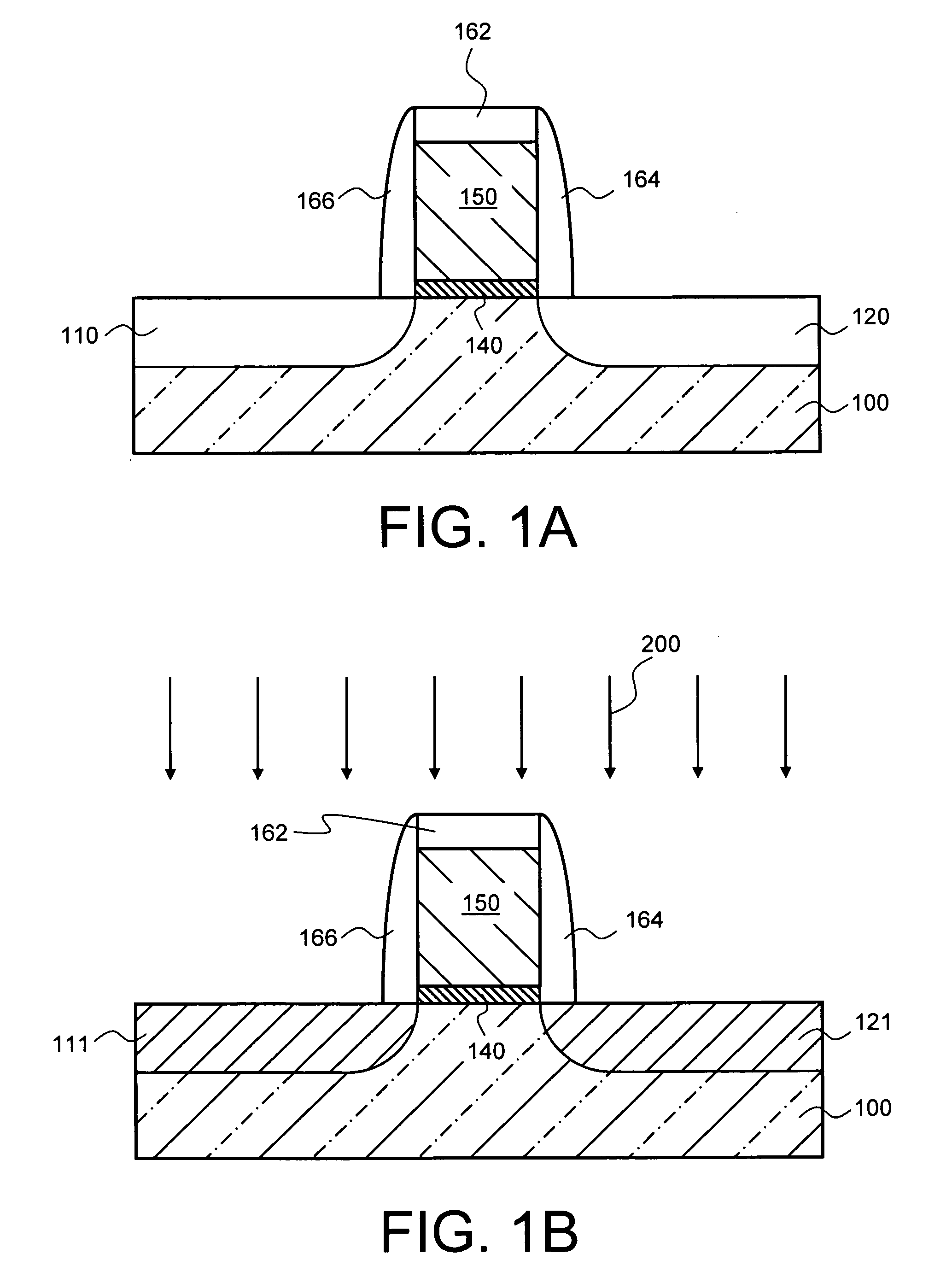
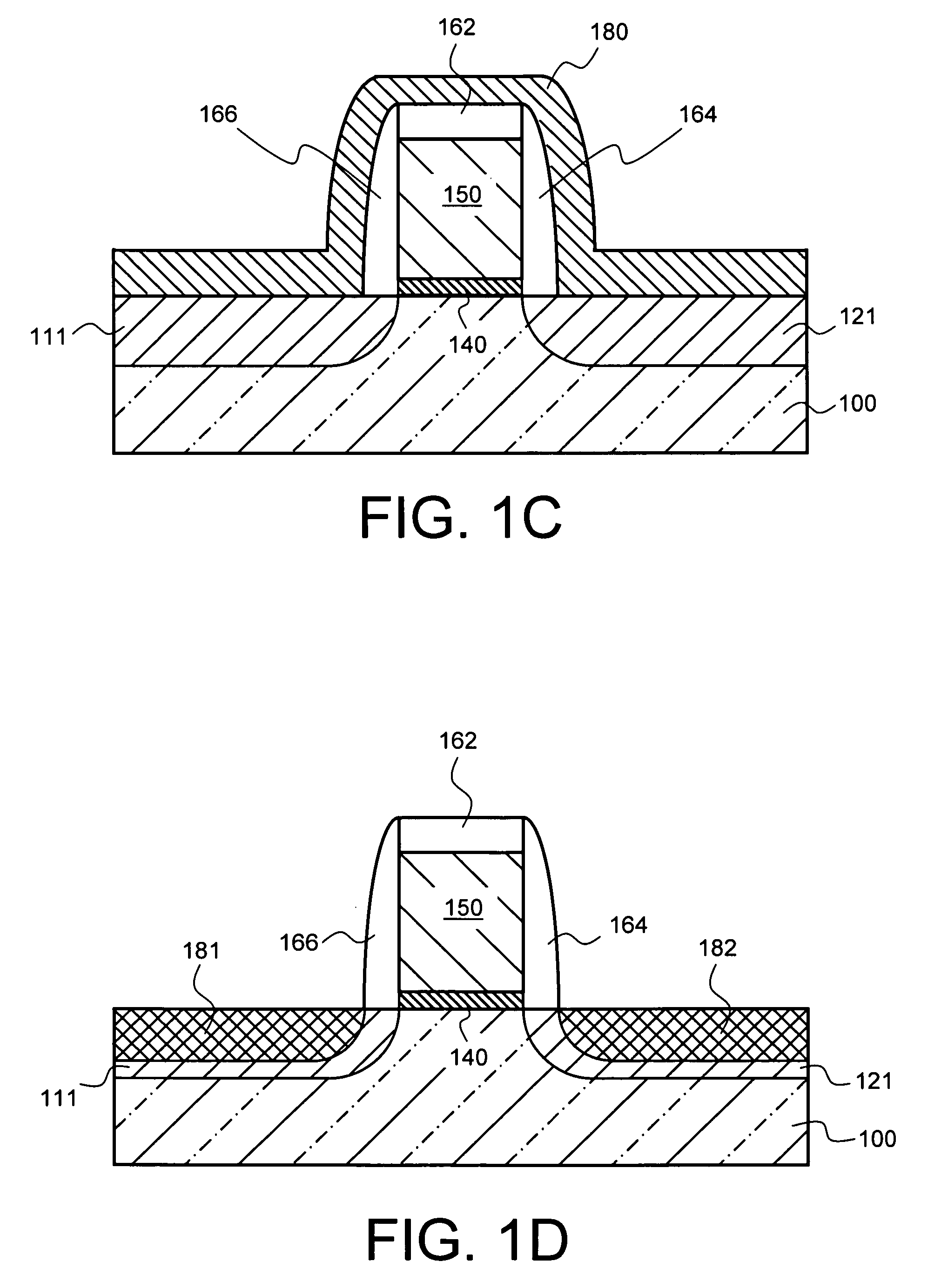
[0011]Embodiments of the present invention describe a method of forming self-aligned low resistance contact layers on a semiconductor device. In an embodiment of the present invention, the semiconductor device comprises a substrate having a source region and a drain region. An amorphous semiconductor layer is then selectively deposited onto each of the source and drain regions by alternatingly exposing the substrate to a first precursor and a second precursor. In one embodiment, the substrate is alternatingly exposed to the first and second precursors by using a plasma enhanced che...


PUM


Abstract

Embodiments of the present invention describe a method of fabricating low resistance contact layers on a semiconductor device. The semiconductor device comprises a substrate having source and drain regions. The substrate is alternatingly exposed to a first precursor and a second precursor to selectively deposit an amorphous semiconductor layer onto each of the source and drain regions. A metal layer is then deposited over the amorphous semiconductor layer on each of the source and drain regions. An annealing process is then performed on the substrate to allow the metal layer to react with amorphous semiconductor layer to form a low resistance contact layer on each of the source and drain regions. The low resistance contact layer on each of the source and drain regions can be formed as either a silicide layer or germanide layer depending on the type of precursors used.

Description

BACKGROUND OF THE INVENTION[0001]1. Field of the Invention[0002]The present invention relates to the field of semiconductor processing and more particularly to a method of forming self-aligned low resistance contact layers on a semiconductor device.[0003]2. Discussion of Related Art[0004]Low resistance contact layers, such as salicides, are commonly used to improve the performance of semiconductor devices, for example the transistor. Typically, the fabrication of salicides on a transistor involves the formation of self-aligned silicide layers on the source and drain regions. One of the advantages of using salicides is to improve the parasitic resistance in the source and drain diffusion regions that often results from the downscaling of source and drain dimensions.[0005]FIGS. 1A-1D illustrate a conventional method of forming salicides on a typical transistor. Referring to FIG. 1A, the transistor comprises a substrate 100 having a gate dielectric layer 140 formed thereon. A poly-sili...

Claims


Application Information

Patent Timeline
IPC IPC(8): H01L21/336
CPCH01L21/02532H01L21/02592H01L21/0262H01L21/02636H01L29/41783H01L21/28525H01L21/28556H01L29/41775H01L21/28518
Inventor RACHMADY, WILLYKLAUS, JASON W.PILLARISETTY, RAVIMUKHERJEE, NILOYKAVALIEROS, JACKKING, SEAN
Owner INTEL CORP
Why Eureka
Try Eureka