Semiconductor devices and methods of manufacture thereof

a technology of semiconductors and semiconductors, applied in the field of semiconductor devices, can solve the problems of reducing the size of bulk semiconductor devices, reducing the manufacturing efficiency of multiple gate transistors such as finfets, and reducing the manufacturing efficiency of multiple gate transistors

Active Publication Date: 2012-02-28
INFINEON TECH AG
View PDF4 Cites 14 Cited by
  • Summary
  • Abstract
  • Description
  • Claims
  • Application Information

AI Technical Summary

Problems solved by technology

Scaling down bulk devices in size has limitations, because of an increase in dopant fluctuations and stronger parasitic short channel effects, due to lack of potential control in the channel region and the deep substrate.
However, multiple gate transistors such as FinFETs are more difficult and complicated to manufacture than planar CMOS devices, and they require distinctly different materials and introduce a variety of processing challenges.
However, it is difficult to find materials, device structures, and manufacturing processes that achieve a symmetric threshold voltage Vt as devices are made smaller, and more particularly for advanced transistor designs having multiple gates.

Method used


Image

  • Semiconductor devices and methods of manufacture thereof
  • Semiconductor devices and methods of manufacture thereof
  • Semiconductor devices and methods of manufacture thereof

Examples


Embodiment Construction

[0019]The making and using of the presently preferred embodiments are discussed in detail below. It should be appreciated, however, that the present invention provides many applicable inventive concepts that can be embodied in a wide variety of specific contexts. The specific embodiments discussed are merely illustrative of specific ways to make and use the invention, and do not limit the scope of the invention.

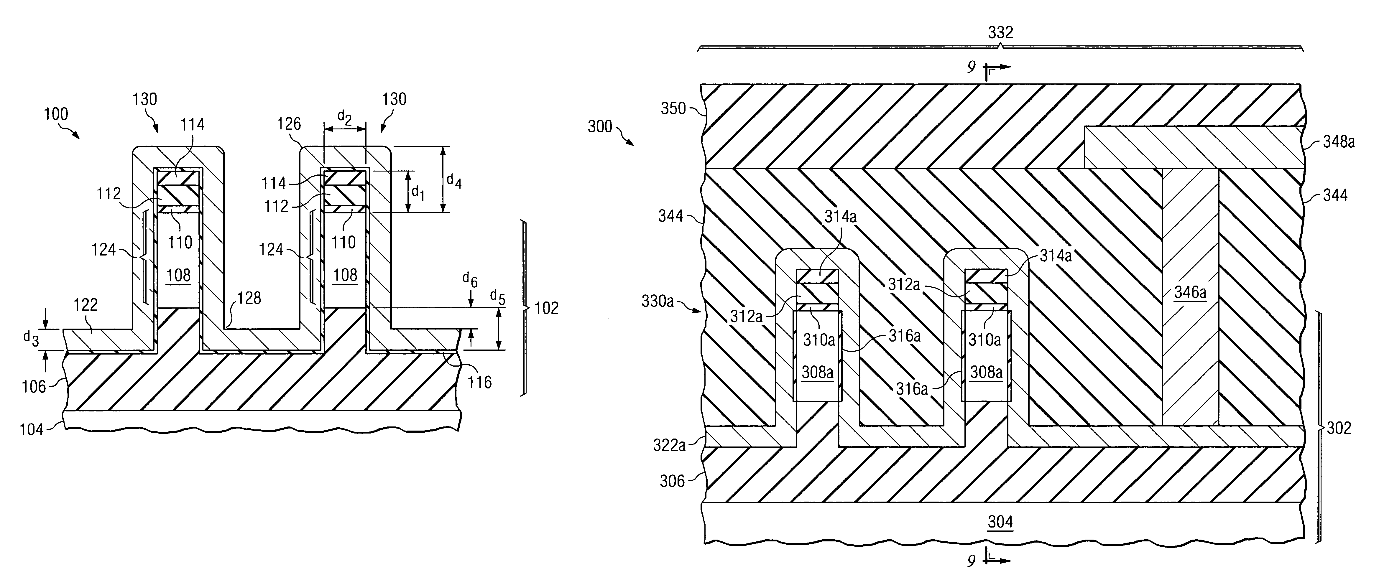
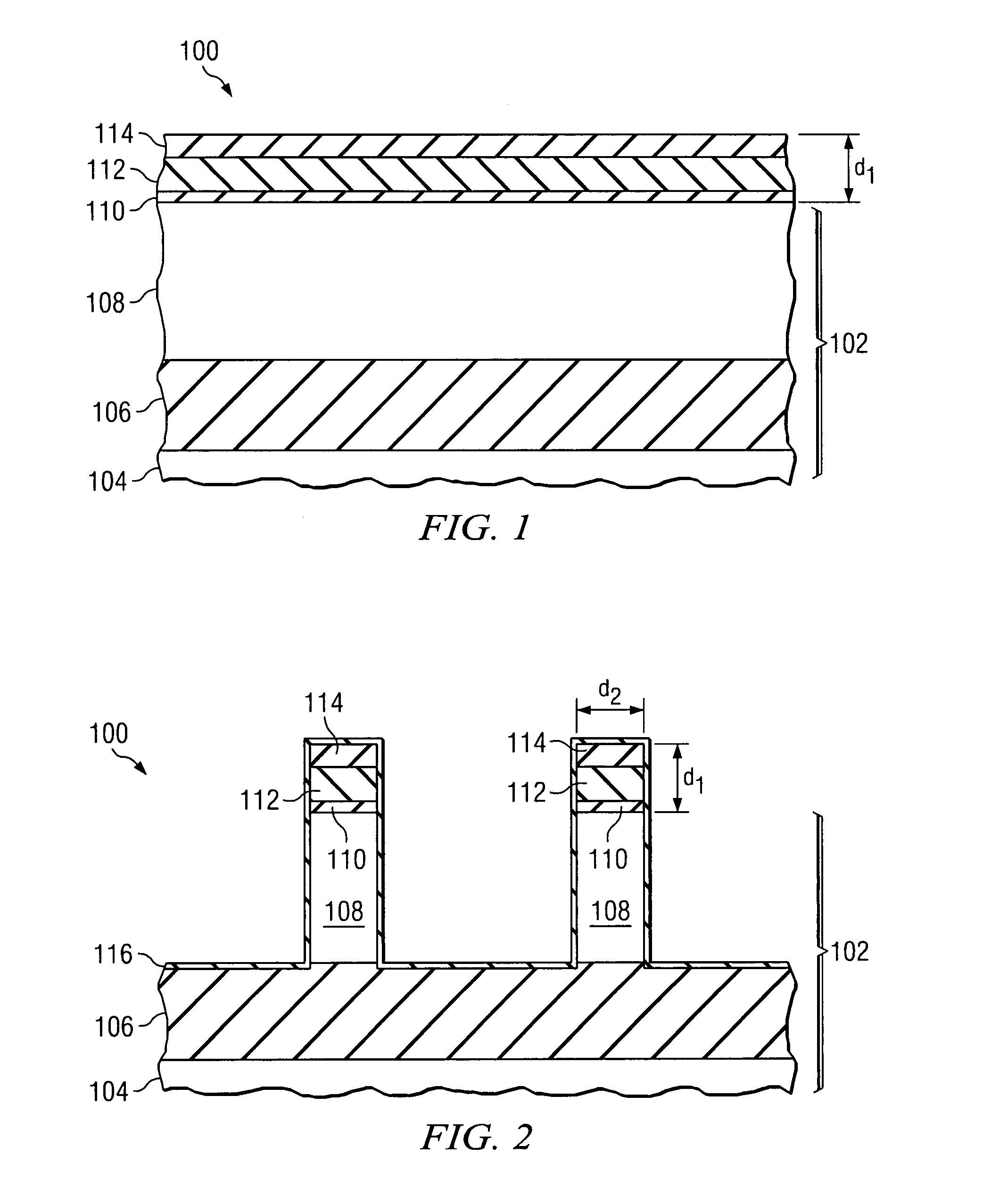
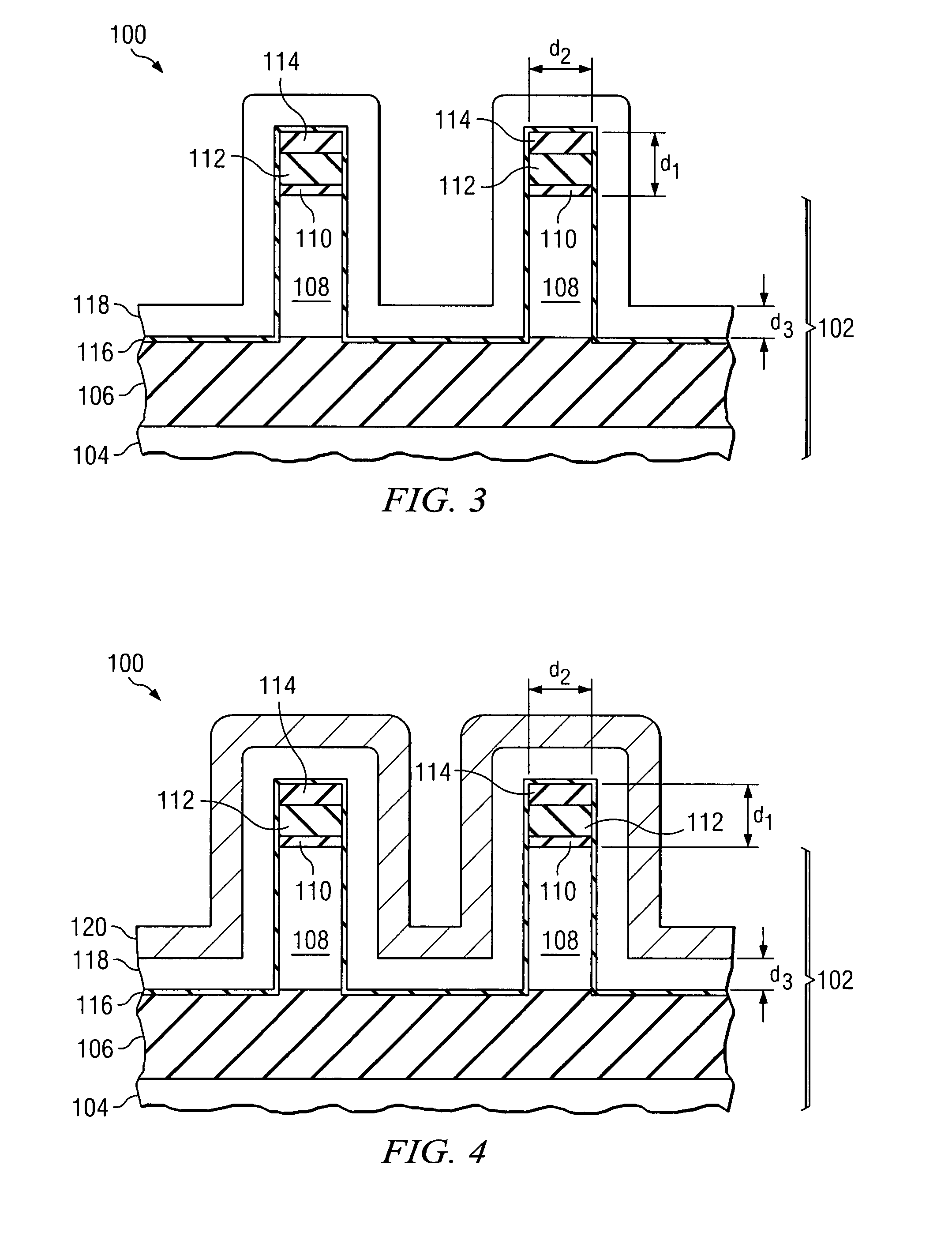
[0020]What are needed in the art are metal gate electrode materials and methods of formation thereof that have a suitable work function for multiple gate CMOS devices. For CMOS FinFET technology to provide a maximum performance benefit over bulk-Si CMOS technology, one issue that needs to be resolved is the development of a tunable work function gate technology for threshold voltage Vt control.

[0021]Because a FinFET controls the channel region by two gates disposed on both sides of a very thin fin of vertical silicon film, a FinFET device requires near mid-gap work functions ...


PUM


Abstract

Semiconductor devices and methods of manufacture thereof are disclosed. In a preferred embodiment, a method of manufacturing a semiconductor device includes forming a transistor, the transistor including a fin having a first side and a second side opposite the first side. The transistor includes a first gate electrode disposed on the first side of the fin and a second gate electrode disposed on the second side of the fin. The method includes forming a silicide or germanide of a metal on the first gate electrode and the second gate electrode of the transistor. The amount of the metal of the silicide or germanide is substantially homogeneous over the first gate electrode and the second gate electrode proximate the fin.

Description

TECHNICAL FIELD[0001]The present invention relates generally to semiconductor devices, and more particularly to transistors having multiple gates and methods of manufacture thereof.BACKGROUND[0002]Semiconductor devices are used in a variety of electronic applications, such as personal computers, cell phones, digital cameras, and other electronic equipment, as examples. Semiconductor devices are typically fabricated by sequentially depositing insulating or dielectric layers, conductive layers, and semiconductive layers of material over a semiconductor substrate, and patterning the various layers using lithography to form circuit components and elements thereon.[0003]A transistor is an element that is utilized extensively in semiconductor devices. There may be millions of transistors on a single integrated circuit (IC), for example. A common type of transistor used in semiconductor device fabrication is a metal oxide semiconductor field effect transistor (MOSFET). Conventional MOSFETs...

Claims


Application Information

Patent Timeline
Patent Type & Authority Patents(United States)
IPC IPC(8): H01L21/336
CPCH01L29/66795H01L29/785
Inventor SCHULZ, THOMAS
Owner INFINEON TECH AG
Why Eureka
Try Eureka