Pad structure of circuit board and manufacturing method thereof

A technology for circuit boards and circuit board circuits, which is applied in chemical/electrolytic methods to remove conductive materials, print circuit components, and electrically connect printed components, etc., can solve problems such as high temperature oxidation, poor heat dissipation, etc. Good cooling effect

Inactive Publication Date: 2010-12-15
昆山华升电路板研发基地有限公司
View PDF0 Cites 15 Cited by
  • Summary
  • Abstract
  • Description
  • Claims
  • Application Information

AI Technical Summary

Problems solved by technology

Subsequent customers solder each component to each pad, because the height of the pad is lower than the surface of the circuit board or fl

Method used


Image

  • Pad structure of circuit board and manufacturing method thereof
  • Pad structure of circuit board and manufacturing method thereof
  • Pad structure of circuit board and manufacturing method thereof

Examples


Embodiment

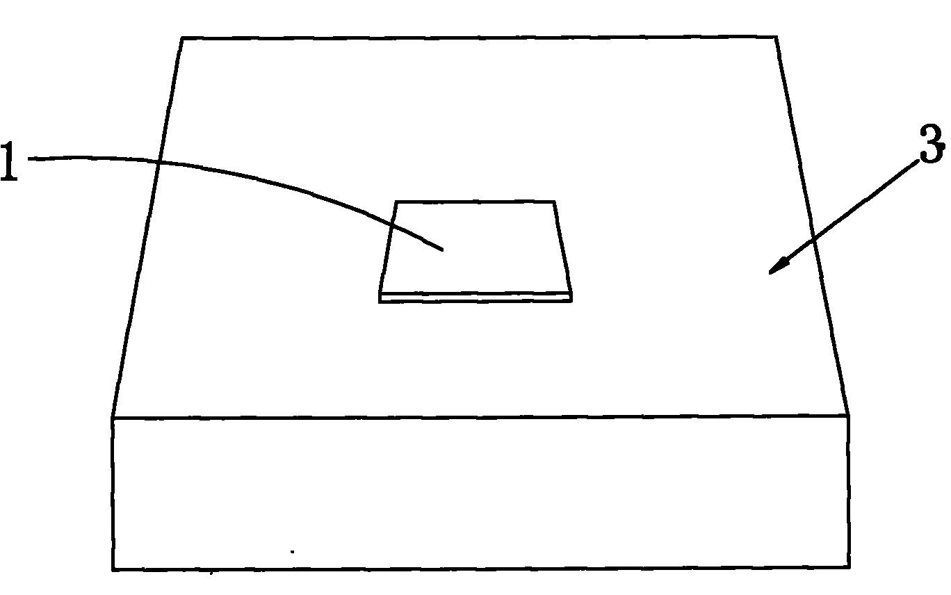
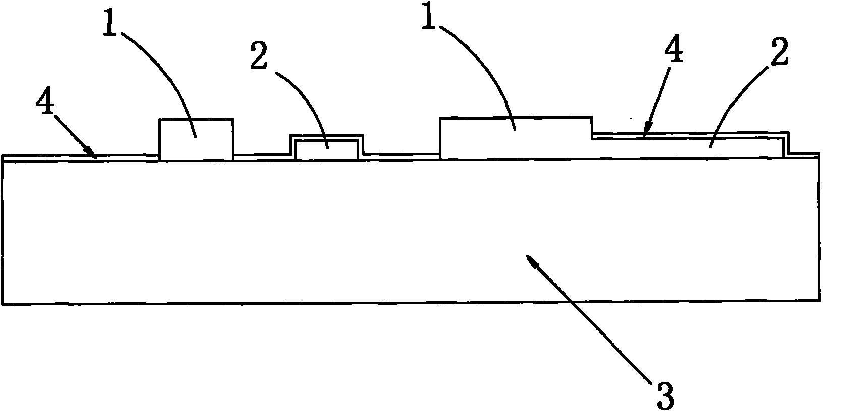
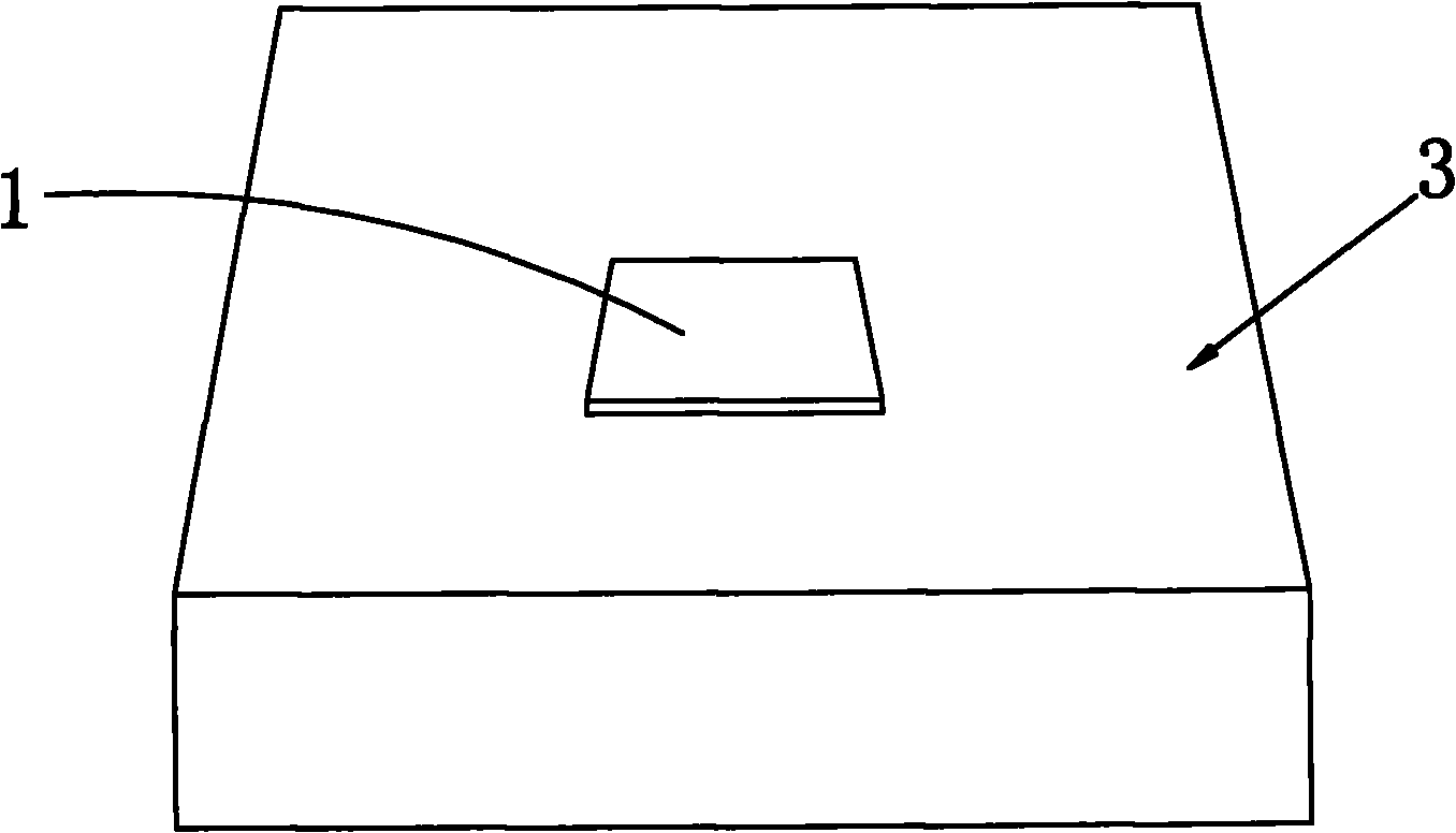
[0018] Embodiment: A pad structure of a circuit board. The circuit board 3 is provided with several pads 1 that are not covered by the solder resist layer 4 on the surface of the circuit board and connected to the circuit board lines 2. The pads 1 are higher than the circuit board. board surface.

[0019] The pad 1 is a metal pad formed by synchronous etching with the circuit board line 2 on the same metal layer closest to the surface of the circuit board, and the realization method that the pad 1 is higher than the surface of the circuit board is: the pad 1 The metal layer of the pad 1 is thicker than the metal layer of the circuit board line 2, and the thickness difference between the metal layer of the pad 1 and the metal layer of the circuit board line 2 is greater than the thickness of the solder resist layer 4 on the surface of the circuit board.

[0020] The realization method that the metal layer of the pad 1 is thicker than the metal layer of the circuit board circuit...


PUM


Abstract

The invention discloses a pad structure of a circuit board and a manufacturing method thereof. The circuit board is provided with a plurality of pads not covered by a solder mask on the surface of the circuit board and connected with the line of the circuit board, and the pads are higher than the surface of the circuit board. The manufacturing method is performed according to the following steps of: a, covering a protection layer at the pad position of an outer metal layer of the circuit board according to the design; b, thinning the outer metal layer not covered by the protection layer for set thickness by using a micro etching technology; c, washing off the protection layer, and performing the subsequent etching technology of the line and the pad of the circuit board according to the design to manufacture the line and the pad of the circuit board; d, performing a solder resisting technology according to the design to enable the solder mask to cover the line of the circuit board, wherein the thinned set thickness of the outer metal layer in the step b is greater than the thickness of the solder mask in the step d. As the pads are higher than the surface of the circuit board, after the subsequent client correspondingly solders each element to each pad, the weld between the element and the circuit board has good heat dissipation so that high-temperature oxidation is not easy to happen during use.

Description

technical field [0001] The invention relates to a circuit board structure and a manufacturing method thereof, in particular to a circuit board pad structure and a manufacturing method thereof. Background technique [0002] The pads and lines of the existing circuit boards are formed by etching on the same thickness of copper foil. The pad height is generally below or flush with the surface of the circuit board. Subsequent customers soldered each component to each pad, because the height of the pad is lower than the surface of the circuit board or flush with the surface of the circuit board, the heat dissipation is poor, and high temperature oxidation is more likely to occur during use. Contents of the invention [0003] In order to overcome the above-mentioned defects, the present invention provides a pad structure of a circuit board and a manufacturing method thereof, which can achieve a higher heat dissipation effect. [0004] The technical scheme that the present inve...

Claims


Application Information

Patent Timeline
IPC IPC(8): H05K1/11H05K3/06
Inventor 黄坤唐雪明曹庆荣
Owner 昆山华升电路板研发基地有限公司
Why Eureka
Try Eureka