Steel mesh and PCB (Printed Circuit Board)

A technology for printed circuit boards and stencils, which is applied to printed circuit components, printed circuits assembled with electrical components, printed circuits connected with non-printed electrical components, etc., which can solve the problem of wasting solder paste, high solder paste cost, component Problems such as position offset, suspension bridge, bridge, etc., achieve the effect of reducing soldering time, saving solder paste, and balancing tension

Inactive Publication Date: 2010-12-22
SHENZHEN H&T INTELLIGENT CONTROL
View PDF4 Cites 17 Cited by
  • Summary
  • Abstract
  • Description
  • Claims
  • Application Information

AI Technical Summary

Problems solved by technology

[0003] In reflow soldering, when the solder paste reaches the melting temperature, under the action of balanced surface tension, it will produce a self-positioning effect. And the characteristics of "self-positioning effect", the reflow soldering process has stricter requirements on pad design and component standardization. If the surface tension of the molten solder paste is unbalanced, component position deviation, suspension bridges, bridges, etc. will occur after soldering. Defects, more solder paste is wasted, and the cost of solder paste is relatively high

Method used


Image

  • Steel mesh and PCB (Printed Circuit Board)
  • Steel mesh and PCB (Printed Circuit Board)
  • Steel mesh and PCB (Printed Circuit Board)

Examples


Embodiment Construction

[0021] It should be understood that the specific embodiments described here are only used to explain the present invention, not to limit the present invention.

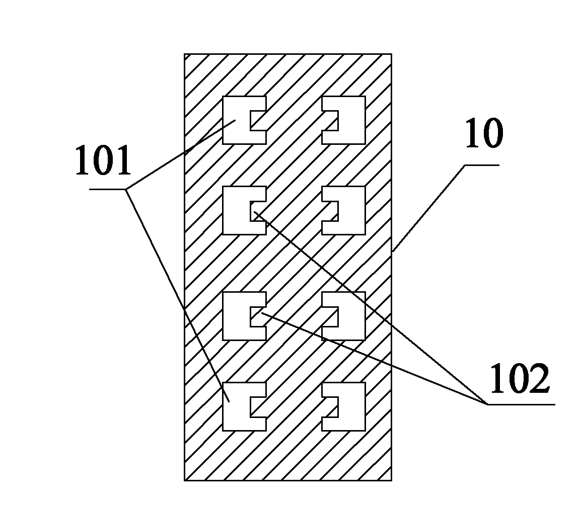
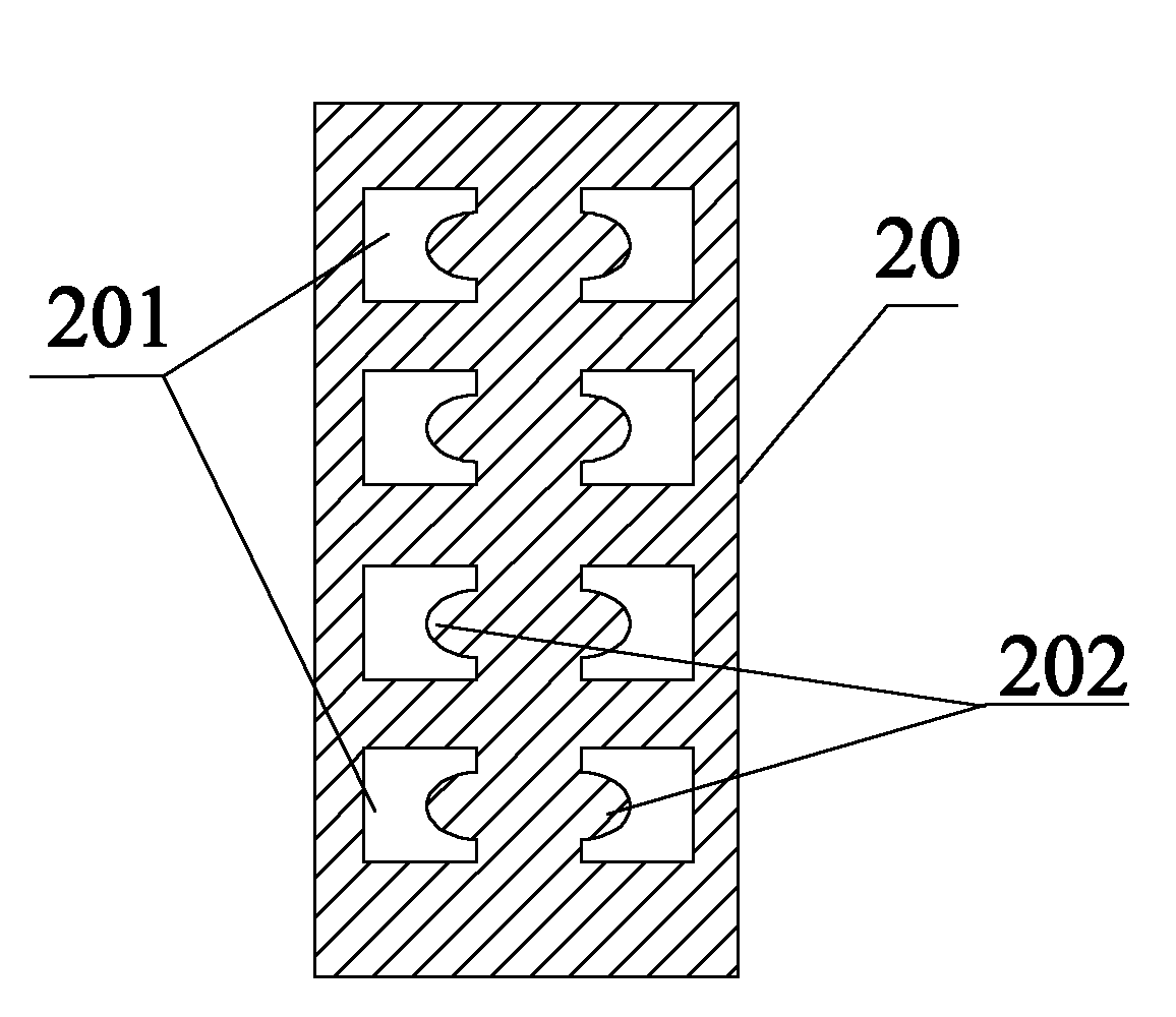
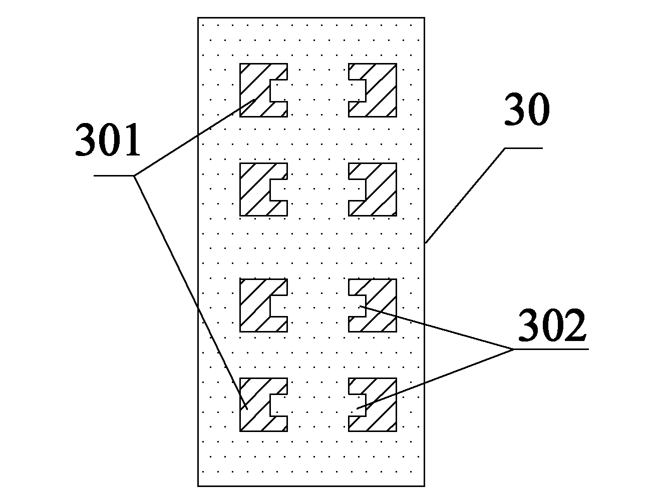
[0022] refer to Figure 1a , an embodiment of a stencil of the present invention is proposed, a plurality of holes 101 are provided on the stencil 10, and at least one bump 102 is arranged in the hole 101. In this embodiment, the above-mentioned bump 102 is set It is one, and the hole 101 is in the shape of "concave" after the protrusion 102 is set.

[0023] In the above embodiment, the shapes of the protrusions 102 provided in each of the holes 101 may be the same or different, that is, the shapes of the holes 101 provided on the same steel mesh 10 may be the same or not completely the same. In this embodiment The holes 101 are set to have the same shape and are symmetrically set on the steel mesh, and can be located in the middle inner position, and set according to actual application conditions.

[0024] Applying ...


PUM


Abstract

The invention discloses a steel mesh which is provided with a plurality of holes, wherein at least one protrusion is arranged in one hole. The invention also discloses a PCB (Printed Circuit Board) which is provided with a plurality of bonding pads, wherein the bonding pads are provided with at least one notch, and the shape of each hole of the steel mesh is matched with the shape of each bonding pad. Limited by the protrusions in the steel mesh holes, the quantity of dipped solder paste is reduced to achieve the aim of reducing the consumption of the solder paste at the bottom of an element or a device, the internal flowing of the solder paste is lessened by the reduced consumption of the solder paste so that the surface tension of the element or the device is balanced to avoid adverse phenomena, such as tin wires and tombstones generated at the bottom of the element or the device, the rotating position offset of the element or the device during the reflow, and the like.

Description

technical field [0001] The invention relates to a steel mesh and a printed circuit board, in particular to a material-saving steel mesh and a printed circuit board. Background technique [0002] SMT (Surface Mounted Technology, Surface Mount Technology or Surface Mount Technology) is currently the most popular technology and process in the electronics assembly industry. In the SMT process, the stencil is opened according to the size of the pad 1:1, and the solder paste is usually printed on the PCB (Printed Circuit Board, printed circuit board) with a size of 1:1 with the stencil. The assembly quality of SMT It has a direct and very important relationship with the PCB pad design. If the PCB pad design is correct, a small amount of skew during mounting can be corrected due to the surface tension of the molten solder during reflow soldering (called self-positioning or self-positioning). Correction effect); On the contrary, if the PCB pad design is not correct, even if the mou...

Claims


Application Information

Patent Timeline
Patent Type & Authority Applications(China)
IPC IPC(8): H05K3/34H05K1/11H05K1/18
Inventor 袁天龙
Owner SHENZHEN H&T INTELLIGENT CONTROL
Why Eureka
Try Eureka